Organic electroluminescent display, and prepartion method

A luminescent and display technology, applied in the field of organic electroluminescent display, can solve the problems affecting the luminous brightness of light-emitting devices, the difference of current value, the uneven luminous brightness of the display, etc., achieve the improvement of display brightness and display uniformity, and broad application prospects , The effect of reducing the column lead resistance

Active Publication Date: 2007-02-21
KUNSHAN VISIONOX DISPLAY TECH
View PDF0 Cites 11 Cited by
  • Summary
  • Abstract
  • Description
  • Claims
  • Application Information

AI Technical Summary

Problems solved by technology

[0004] However, since the resistance of the ITO lead area far away from the light-emitting area in the light-emitting area is very different from the resistance of the ITO lead area outside the light-emitting area, that is, the resistance of the area far away from the ITO lead is large, and the resistance of the area close to the ITO lead is small. The current value flowing through different areas has a big difference, and the current value affects the luminous brightness of the organic electroluminescent device, causing the area with large resistance and low current to be darker than the area with small resistance and high current during image display, resulting in the luminous brightness of the display Uneven, it is difficult to achieve high display quality (ITO leads refer to the leads located outside the light-emitting area for connecting the internal electrodes of the light-emitting area to the external driver chip)

Method used


Image

  • Organic electroluminescent display, and prepartion method
  • Organic electroluminescent display, and prepartion method
  • Organic electroluminescent display, and prepartion method

Examples


Embodiment 1

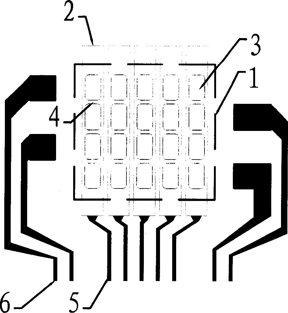
[0042] figure 2 Preparation process of the auxiliary electrode shown. (The preparation process is carried out in the purification workshop). The glass substrate is cleaned with UV irradiation and lotion containing surfactant in sequence. A layer of ITO is sputtered on the cleaned glass substrate to form a transparent electrode. The resistance of the transparent electrode is 15Ω. The ITO film thickness is 170nm, and a layer of metal chromium is sputtered on the cleaned ITO substrate with a thickness of 100-200nm. Make a mask so that the pattern obtained by exposure of the mask includes all the patterns in the gap area 4 except the light-emitting pixels 3 on the first electrode 2 in the light-emitting region 1 and the patterns of the transparent electrode leads 5 and 6 outside the light-emitting region. Apply the photosensitive adhesive evenly on the chromium metal layer on the surface of the glass substrate, put the photosensitive adhesive coated glass substrate into a high-t...

Embodiment 2

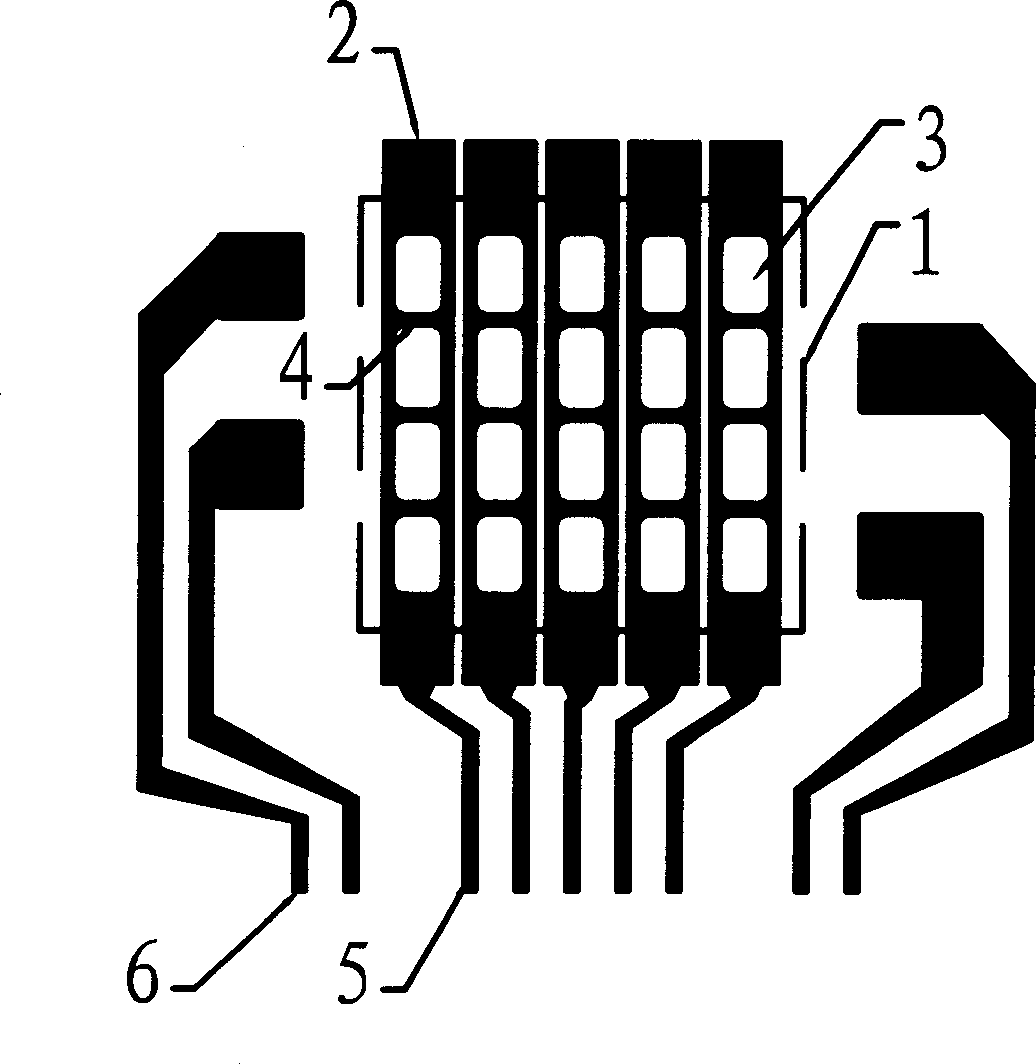
[0044] image 3 The preparation process of the shown auxiliary electrode, the specific operation process is the same as that of Example 1, the difference lies in the making of the mask plate and the selection of aluminum as the low-resistance metal, image 3 The mask plate made in the process, so that the exposed pattern of the mask plate includes the light-emitting pixel gap area 4 pattern spaced on the transparent electrode 2 in the light-emitting area 1 and the transparent electrode lead wires 5 and 6 patterns outside the light-emitting area, and finally made The auxiliary electrode pattern such as image 3 shown.

Embodiment 3

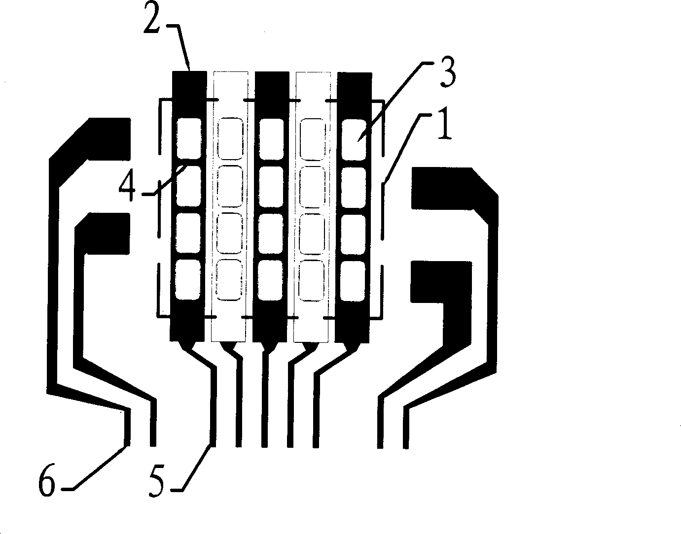
[0046] Figure 4 In the preparation process of the organic electroluminescent display shown in Example 1, on the basis of the auxiliary electrode obtained in Example 1, the pattern transfer and etching of the ITO electrode are carried out, and a group of parallel and separated straight lines are photoetched. Spin-coat a layer of photosensitive organic insulating material, which can be photosensitive PI, positive novolac photoresist, negative cyclized rubber, etc. In this embodiment, photosensitive PI is selected, exposed before baking, and the exposure pattern is mesh structure (only the light-emitting area of ​​the device pixel and the lead connection area are exposed) or a strip structure (a group of parallel and separated straight lines perpendicular to the transparent electrode pattern), the width of the line is determined by the display resolution. Determined by the spacing between pixels, the line width is 10-50um. The above-mentioned exposed organic insulating layer is...


PUM

PropertyMeasurementUnit
Resistanceaaaaaaaaaa
Thicknessaaaaaaaaaa

Abstract

The display includes transparent substrate, first electrode, organic functional layer, second electrode, and auxiliary electrode setup on first electrode. The auxiliary electrode includes the covering metal layer in low resistance on column lead wire and row lead wire of transparent electrode outside zone of luminosity. Characters are that the auxiliary electrode further includes the covering metal layer in low resistance inside gap area of luminescence pixels on first electrode inside zone of luminosity. Resistance of the metal in low resistance is smaller than resistance of first electrode. The first electrode is a transparent electrode. Reducing difference of resistance between resistance of column lead wire and resistance of different area inside zone of luminosity effectively, the disclosed display of organic electroluminescence improves display brightness and display evenness.

Description

technical field [0001] The invention relates to the field of organic electroluminescence display, in particular to an auxiliary electrode of an organic electroluminescence display, an organic electroluminescence display and a preparation method thereof. Background technique [0002] Organic Electroluminescent Devices (Organic Electroluminescent Devices, hereinafter referred to as OLED) are luminous bodies formed by evaporating organic electroluminescent materials on the first electrode (anode) and then covering the second electrode (cathode). The first electrode is transparent The electrodes are mainly composed of metal oxides such as indium tin oxide (ITO), tin zinc oxide, or metals with a high work function. Usually in passive OLED production, the anode is used as the column lead, and the cathode is used as the row lead to connect to the external lead wire, and the signal provided by the driver chip is used for display. [0003] ITO is a commonly used transparent electrod...

Claims


Application Information

Patent Timeline
IPC IPC(8): H01L27/32H01L51/50H01L51/56H01L21/768H01L21/28H05B33/26H05B33/10
Inventor 邱勇徐粤吴延德段练
Owner KUNSHAN VISIONOX DISPLAY TECH
Why Eureka
Try Eureka