Electronic device

A technology of electronic devices and electrodes, which is applied to circuits, antenna supports/mounting devices, printed circuits assembled with electrical components, etc., can solve problems such as hindering cost reduction, and achieve high production efficiency and excellent communication characteristics.

Inactive Publication Date: 2007-02-21
RESONAC CORPORATION
View PDF1 Cites 3 Cited by
  • Summary
  • Abstract
  • Description
  • Claims
  • Application Information

AI Technical Summary

Problems solved by technology

For these electrodes, gold, which has low electrical resistance and good oxidation resistance, has been used frequently, which hinders cost reduction.

Method used


Image

  • Electronic device
  • Electronic device
  • Electronic device

Examples


Embodiment

[0059] Hereinafter, preferred embodiments of the present invention will be described in more detail with reference to the drawings, but the present invention is not limited to these embodiments.

no. 1 Embodiment

[0061] Use below image 3 The first embodiment will be described.

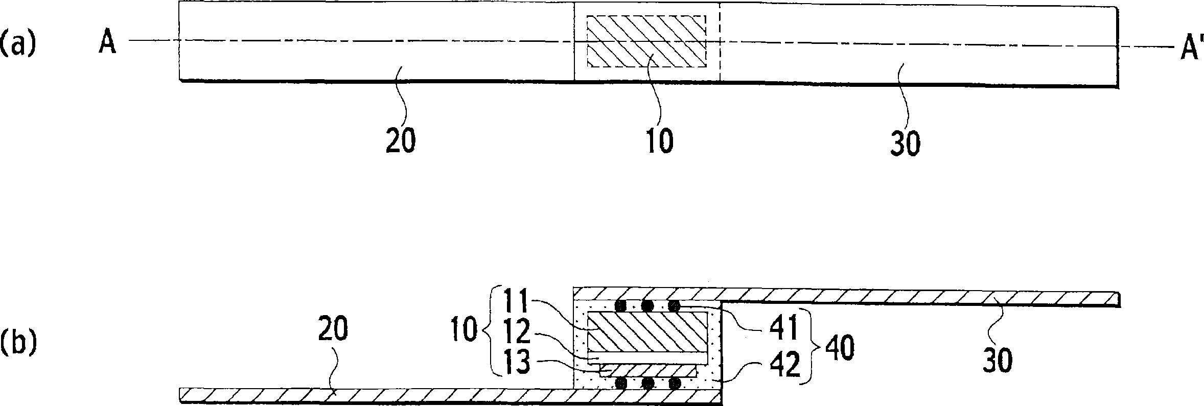
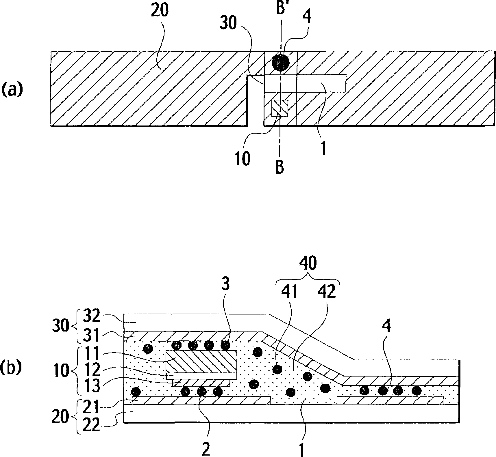
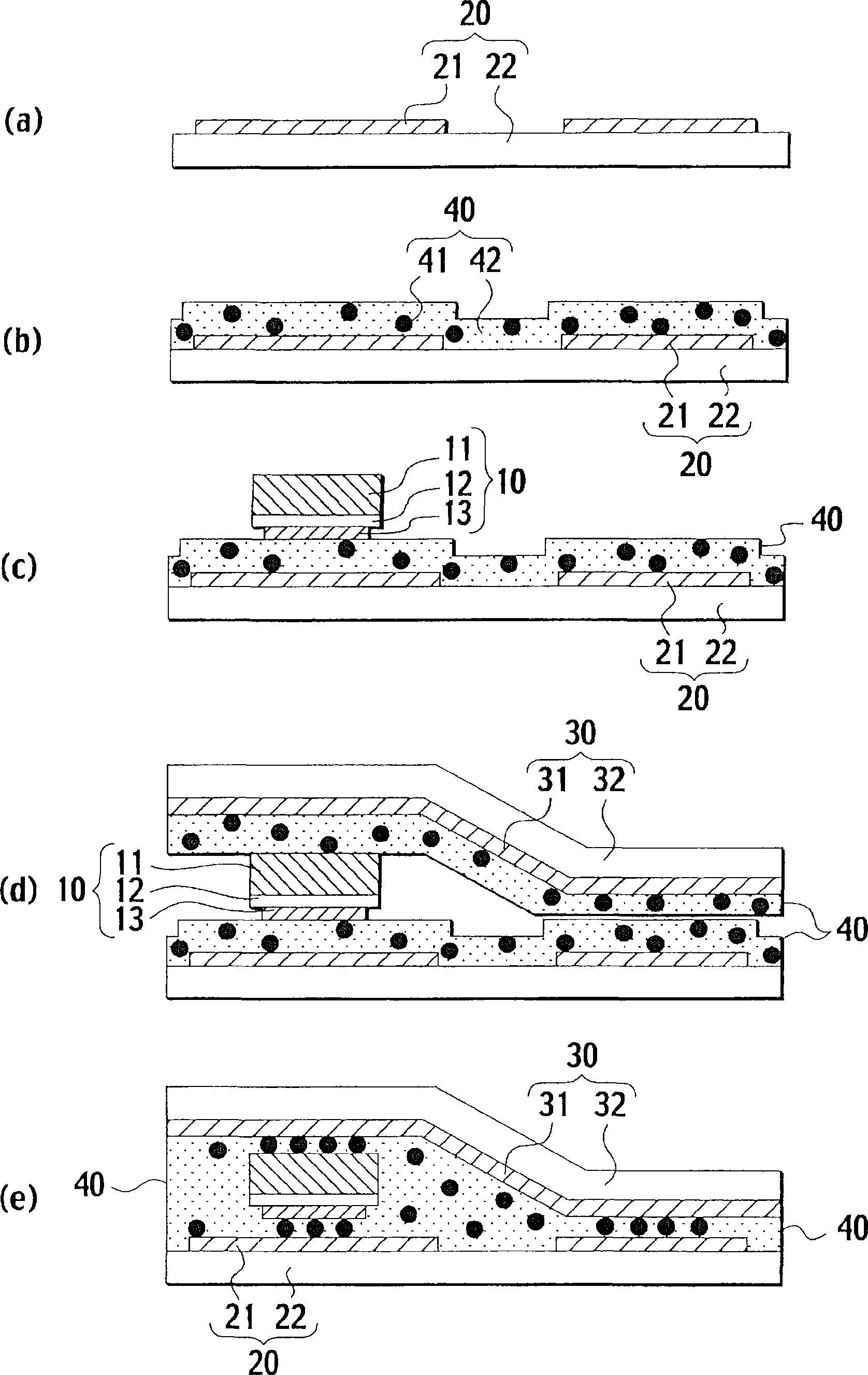
[0062] first as image 3 As shown in (a), on the polyethylene terephthalate base substrate 22 with a thickness of 50 μm, an aluminum foil with a thickness of 9 μm is pasted with an adhesive to form a tape-shaped substrate. Screen printing After the etching protection layer is formed, the antenna circuit 21 is formed by using an aqueous solution of ferric chloride as an etching solution to form the first circuit layer 10 . Here, the antenna width of the antenna circuit 21 is 2.5 mm, and the notch width is 0.5 mm. The accompanying drawings contain the following process steps, represented in figure 2 The cross-section of B-B' when it is cut.

[0063] Secondly, if image 3 As shown in (b), at a specific position on the antenna circuit 21, an anisotropic conductive adhesive film (AC-2052P-45 (manufactured by Hitachi Chemical Industry Co., Ltd.)) with a width of 2mm was laminated at 80°C, and the separator fil...

no. 2 Embodiment

[0070] Below, use Figure 4 The second embodiment will be described.

[0071] First, if Figure 4 As shown in (a), to image 3 (c) Up to now, the above-mentioned first circuit layer 20 is processed by using the same process as that of the first embodiment, and the above-mentioned anisotropic conductive adhesive film is laminated on the antenna circuit to form the anisotropic conductive adhesive layer 40 , and then at a specific position on the antenna circuit 21, the above-mentioned IC element 10 is temporarily fixed.

[0072] Secondly, if Figure 4 As shown in (b), in the IC element 10 described above, a conductive adhesive 50 containing a silver filler is coated on the surface opposite to the surface facing the antenna circuit 21 .

[0073] Secondly, if Figure 4 As shown in (c), on a polyethylene terephthalate base material 32 with a thickness of 50 μm, an aluminum foil with a thickness of 9 μm is attached as a conductive layer 31 with an adhesive to form a tape-shaped...


PUM

PropertyMeasurementUnit
thicknessaaaaaaaaaa

Abstract

Disclosed is an electronic device comprising an IC element 10, a first circuit layer 20 on the surface of which is formed an antenna circuit 21 composed of a conductive layer, and a second circuit layer 30 on the surface of which is formed a conductive layer 31. The IC element 10 comprises a base substrate 11 composed of silicon, a semiconductor circuit layer 12 formed on one side of the base substrate 11 in which layer a semiconductor circuit is formed, and an electrode 13 formed on the semiconductor circuit layer 12. The first circuit layer 20 is connected to either the other side of the base substrate 11 or the electrode 13, and the second circuit layer 30 is electrically connected to either that same other side of the base substrate 11 or the electrode 13 which ever is not connected to the first circuit layer 20. Consequently the electronic device can be efficiently produced at low-cost while achieving good communications properties.

Description

technical field [0001] The invention relates to a non-contact individual identification device loaded with IC components, in particular to an electronic device suitable for obtaining low cost, high production efficiency and good communication characteristics. Background technique [0002] In recent years, non-contact individual identification systems using RFID (Radio Frequency Identificatin) tags have attracted attention in all industries of manufacturing, distribution, and sales as a system for managing the entire life of an item. In particular, radio-based RFID tags using 2.45 GHz microwaves have attracted attention because they have a structure in which an antenna is mounted outside the IC element, enabling a communication distance of several meters. Currently, they are being used in the logistics of a large number of commodities and in the management or manufacture of articles. Build a system for the purpose of history management, etc. [0003] As radio RFID tags using...

Claims


Application Information

Patent Timeline
Patent Type & Authority Applications(China)
IPC IPC(8): G06K19/00H05K3/32H01L21/56H01L21/60B42D15/10C09J9/02C09J201/00G06K19/077H01L23/31H01L23/498H01Q1/22H01Q1/40H01Q23/00H05K1/18
CPCH01L2924/01074H01L2924/01006H01Q1/40H01L23/49855H01L24/33H05K3/323H01L2924/00013H01Q23/00H01L2924/01027H01L2224/2929H01L2924/01015H01L2924/01005H01L2924/01033H01L2924/01047H01L2224/29111H01L2924/01019H01L2924/01079H01L2924/01013H01L2224/83192H01Q1/2208H01L2924/14H01L2924/014H01L2224/29299H01L2924/01078H01L24/29H01L23/3107H01L2924/0105H01L2924/0781H01L2924/3011H01L24/83H01L2924/0132H01L2924/01029H01L2224/293H01L2924/07811G06K19/07749H01L2224/838H05K1/185G06K19/07754G06K19/07786H01L2924/00015H01L2924/00014H01L2224/29099H01L2224/29199H01L2924/00G06K19/07G06K19/02
Inventor 田崎耕司石坂裕宣涩谷正仁田中耕辅新泽正久殿塚秀彦岩田克也
Owner RESONAC CORPORATION
Why Eureka
Try Eureka