Testing facilities for image sensor
An image sensor and test device technology, which can be applied to measurement devices, optical instrument testing, radiation control devices, etc., can solve the problem of insufficient miniaturization of test devices for image sensors, and achieve the effect of miniaturization and cost reduction.
- Summary
- Abstract
- Description
- Claims
- Application Information
AI Technical Summary
Problems solved by technology
Method used
Image

Examples
Embodiment 2
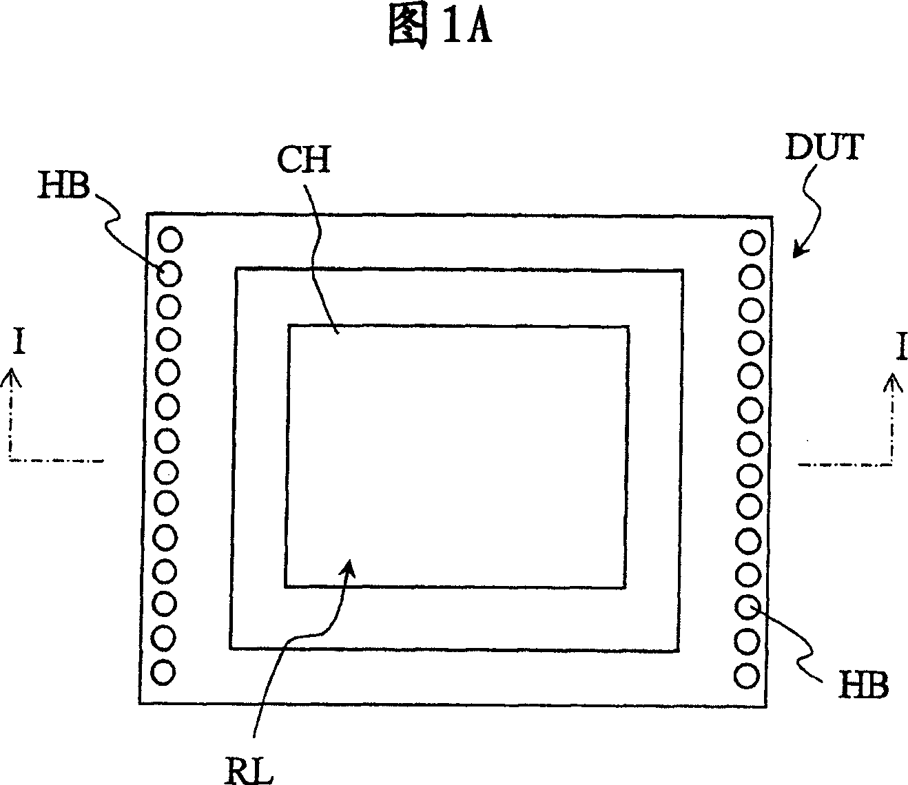
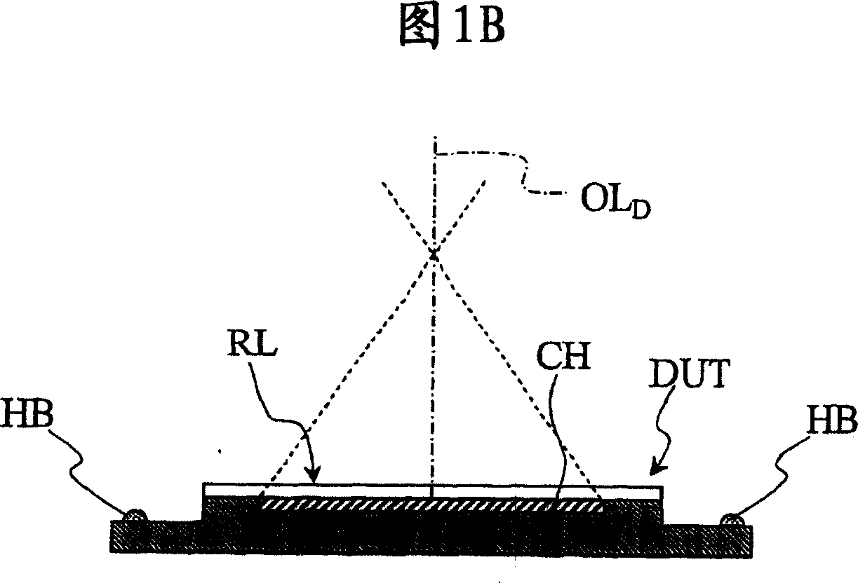
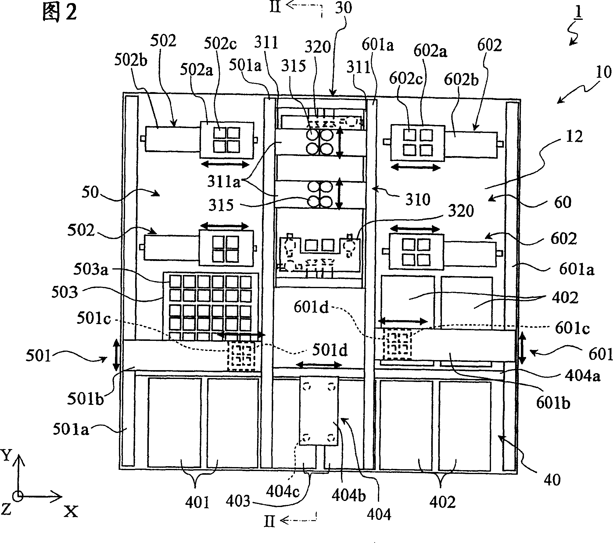
[0322] 34A is a top plan view showing an image sensor as a test object of an image sensor test device according to Embodiment 2 of the present invention, FIG. 34B is a bottom plan view of the image sensor shown in FIG. 34A , and FIG. 34C is a view along VII- 35 is a schematic sectional view showing the contact arm and the test head of the image sensor test device according to Embodiment 2 of the present invention, and FIG. 36 is a schematic sectional view showing the contact of the image sensor test device according to Embodiment 2 of the present invention. 37 is a schematic cross-sectional view of an enlarged upper contact of the contact arm shown in FIGS. 35 and 36 , and FIG. 38 is a plan view of the upper contact shown in FIG. 37 .
[0323] First, in Embodiment 2 of the present invention, when describing the image sensor to be tested, the image sensor DUT', as shown in FIG. 34A to FIG. The CCD sensor or CMOS sensor of the terminal HB is similar to the image sensor DUT of th...
PUM
 Abstract
Description
Claims
Application Information
 - R&D
- Intellectual Property
- Life Sciences
- Materials
- Tech Scout
- Unparalleled Data Quality
- Higher Quality Content
- 60% Fewer Hallucinations
Browse by: Latest US Patents, China's latest patents, Technical Efficacy Thesaurus, Application Domain, Technology Topic, Popular Technical Reports.
© 2025 PatSnap. All rights reserved.Legal|Privacy policy|Modern Slavery Act Transparency Statement|Sitemap|About US| Contact US: help@patsnap.com