Substrate with spacer, panel, liquid crystal panel, method for producing panel, and method for producing liquid crystal panel

A technology of liquid crystal display panels and manufacturing methods, applied in the direction of nonlinear optics, instruments, optics, etc., which can solve problems such as insufficiency, and achieve the effects of preventing damage, reducing temperature changes, and preventing display quality from degrading

Inactive Publication Date: 2007-03-14
SHARP KK
View PDF5 Cites 18 Cited by
  • Summary
  • Abstract
  • Description
  • Claims
  • Application Information

AI Technical Summary

Problems solved by technology

However, the method disclosed in Japanese Patent Laid-Open No. 2001-281678 is not sufficient for the above purpose in consideration of measurement error, accuracy of dripping amount control, and temperature variation

Method used


Image

  • Substrate with spacer, panel, liquid crystal panel, method for producing panel, and method for producing liquid crystal panel
  • Substrate with spacer, panel, liquid crystal panel, method for producing panel, and method for producing liquid crystal panel
  • Substrate with spacer, panel, liquid crystal panel, method for producing panel, and method for producing liquid crystal panel

Examples


no. 1 example

[0080] A liquid crystal display panel and a manufacturing method thereof according to a first embodiment of the present invention will now be described with reference to FIGS. 1A-7B .

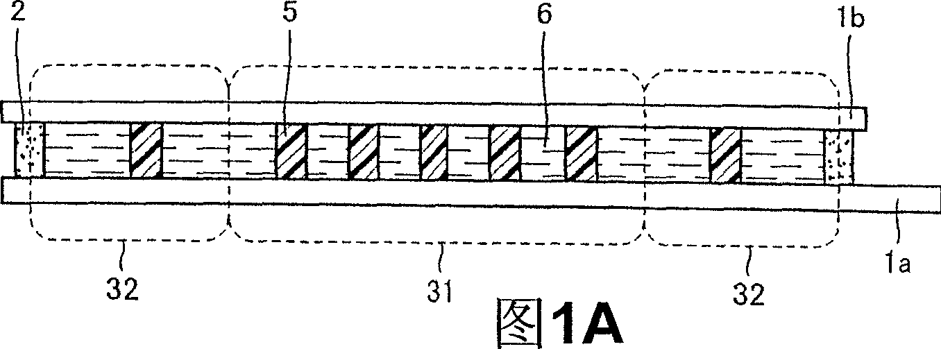
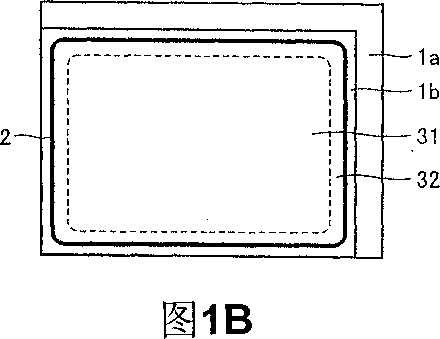
[0081] 1A and 1B show the first liquid crystal display panel of this embodiment. 1A and 1B are a schematic cross-sectional view and a schematic plan view, respectively. As shown in FIG. 1A , two substrates 1 a and 1 b are bonded and fixed together by a sealing member 2 . Drive elements and the like are provided on the main surface of the substrate 1a, and counter electrodes (not shown) and the like are provided on the surface of the substrate 1b. The inner space or area surrounded by the two substrates 1 a and 1 b and the sealing member 2 is hermetically filled with liquid crystal 6 . The substrates 1a and 1b are bonded and fixed together with a space therebetween. Columnar spacers 5 define the distance between the two substrates.

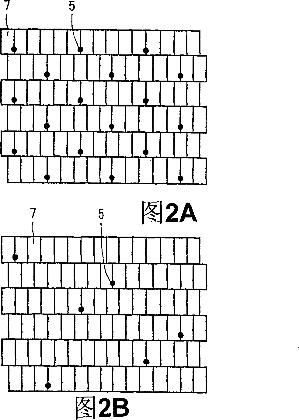
[0082] Columnar spacers 5 are arranged in regions filled w...

no. 2 example

[0102] A description will now be given of a liquid crystal display panel and a method of manufacturing the liquid crystal display panel according to a second embodiment of the present invention with reference to FIGS. 8A and 10 .

[0103] 8A and 8B show the liquid crystal display panel of this embodiment. FIG. 8A is a schematic cross-sectional view, and FIG. 8B is a schematic plan view. As done in the liquid crystal display panel of the first embodiment, the two substrates 1a and 1b are fixed together by the sealing member 2, and the space surrounded by the two substrates 1a and 1b and the sealing member 2 is filled with liquid crystal.

[0104] The liquid crystal display panel of this embodiment includes a low spacer arrangement region 34 near the inner side of the sealing member 2 as a first region, and a high-low spacer arrangement region 33 inside the low spacer arrangement region 34 as a second region. The liquid crystal display panel includes first columnar spacers arra...

no. 3 example

[0122] This embodiment will now be described in conjunction with a substrate with spacers used in a liquid crystal display panel. The substrate with spacers according to the present invention can be used not only in liquid crystal display panels but also in organic EL panels, inorganic EL panels, plasma panels, field emission panels, electrochromic panels, and the like. The liquid crystal panel can be applied not only to a liquid crystal display panel, but also to an image displacement panel that optically shifts pixel positions sequentially, and a parallax barrier panel that can display three-dimensional images. The image displacement panel includes at least one set of liquid crystal panels modulating the polarization states of light emitting elements and birefringent elements combined with the liquid crystal panel for shifting an optical path according to the polarization state of light from the liquid crystal panel. The parallax barrier panel is combined with an image displ...


PUM

PropertyMeasurementUnit
diameteraaaaaaaaaa

Abstract

A liquid crystal display panel includes two substrates (1a and 1b) fixed together by a seal member (2) with their main surfaces opposed to each other, liquid crystal (6) sealingly stored in a region surrounded by the two substrates (1a and 1b) and the seal member (2), and a plurality of columnar spacers (5) arranged in a region surrounded by the two substrates (1a and 1b) and the seal member (2). A number density of the columnar spacers (2) in a low-density region (32) near the inner side of the seal member (2) is smaller than that in a high-density region (31) inside the low-density region (32). The substrate with the spacer has the substrate and the spacer formed on the substrate. The spacer has at least a first spacer portion, and a second spacer portion formed above the first spacer portion. An upper portion of the first spacer has a larger diameter than a bottom of the second spacer portion.

Description

technical field [0001] The invention relates to a liquid crystal display panel and a manufacturing method thereof, in particular to a liquid crystal display panel including column spacers and a manufacturing method thereof. [0002] The invention also relates to a substrate provided with spacers arranged on the substrate. The substrate with the spacer according to the present invention is bonded to the opposite substrate so that a constant interval can be maintained between the substrates. Background technique [0003] The liquid crystal display panel includes a substrate provided with driving elements for driving liquid crystals, and a substrate provided with counter electrodes facing each other, and these substrates are bonded together with their main surfaces facing each other with an interval of several micrometers therebetween. [0004] FIG. 11 is a schematic cross-sectional view of a liquid crystal display panel according to the prior art. For simplicity, FIG. 11 doe...

Claims


Application Information

Patent Timeline
Patent Type & Authority Applications(China)
IPC IPC(8): G02F1/1339
Inventor 横山直人臼仓奈留
Owner SHARP KK
Why Eureka
Try Eureka