Multilayer wiring board and fabricating method of the same

A multi-layer wiring and manufacturing method technology, which is applied in the direction of multi-layer circuit manufacturing, metal pattern materials, electrical connection printing components, etc., can solve the problems of complex board production process, etc., and achieve the effect of uniform structure and high connection stability

Inactive Publication Date: 2007-03-21
SONY CORP
View PDF3 Cites 12 Cited by
  • Summary
  • Abstract
  • Description
  • Claims
  • Application Information

AI Technical Summary

Problems solved by technology

However, integrated boards are produced based on the so-called sequential multilayer wiring technology in

Method used


Image

  • Multilayer wiring board and fabricating method of the same
  • Multilayer wiring board and fabricating method of the same
  • Multilayer wiring board and fabricating method of the same

Examples


Example Embodiment

[0033] The technical solution of the present invention will be described in detail with reference to the accompanying drawings.

[0034] Structure of a multilayer wiring board

[0035] FIG. 3 is a diagram schematically showing a cross section of the multilayer wiring board 10 according to one aspect of the present invention.
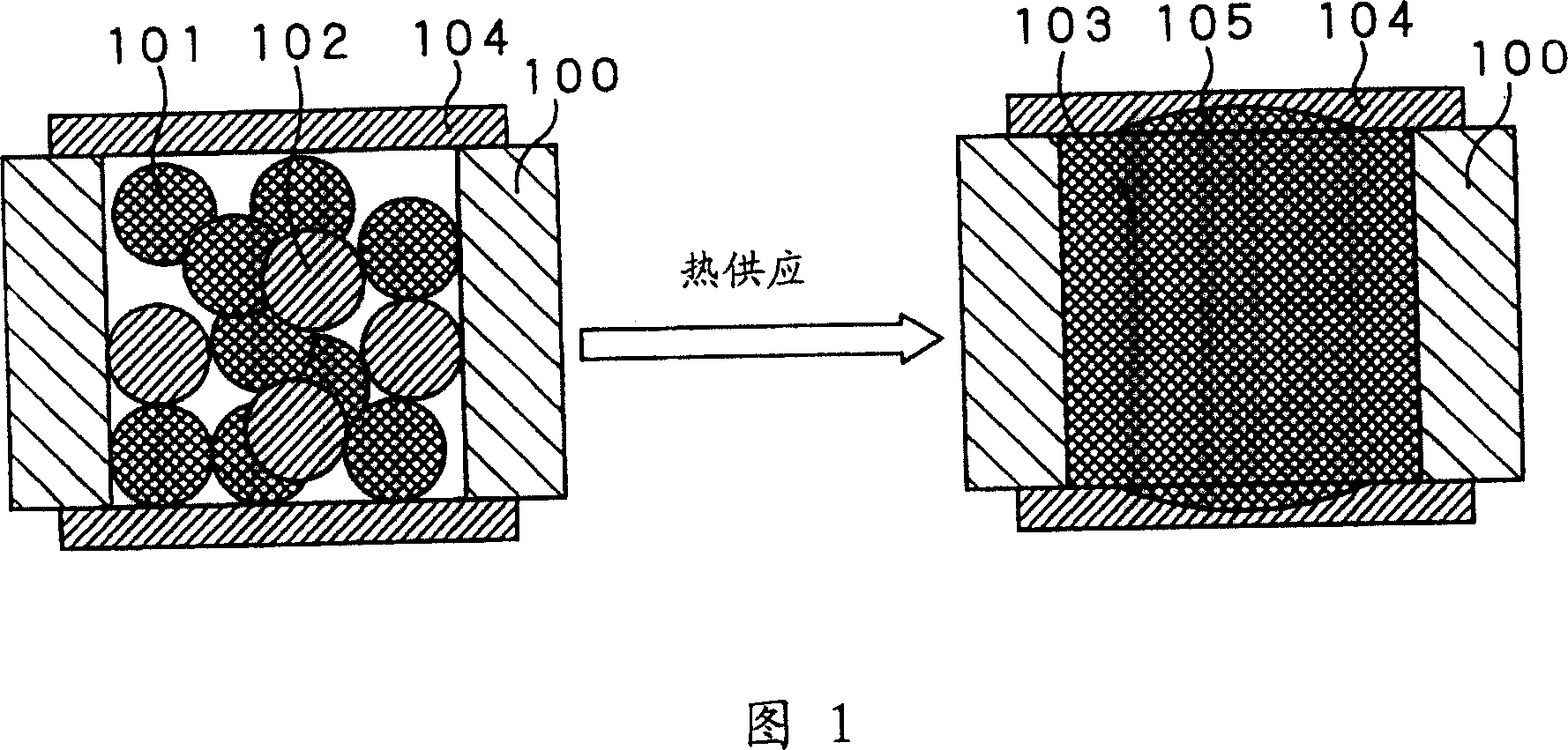
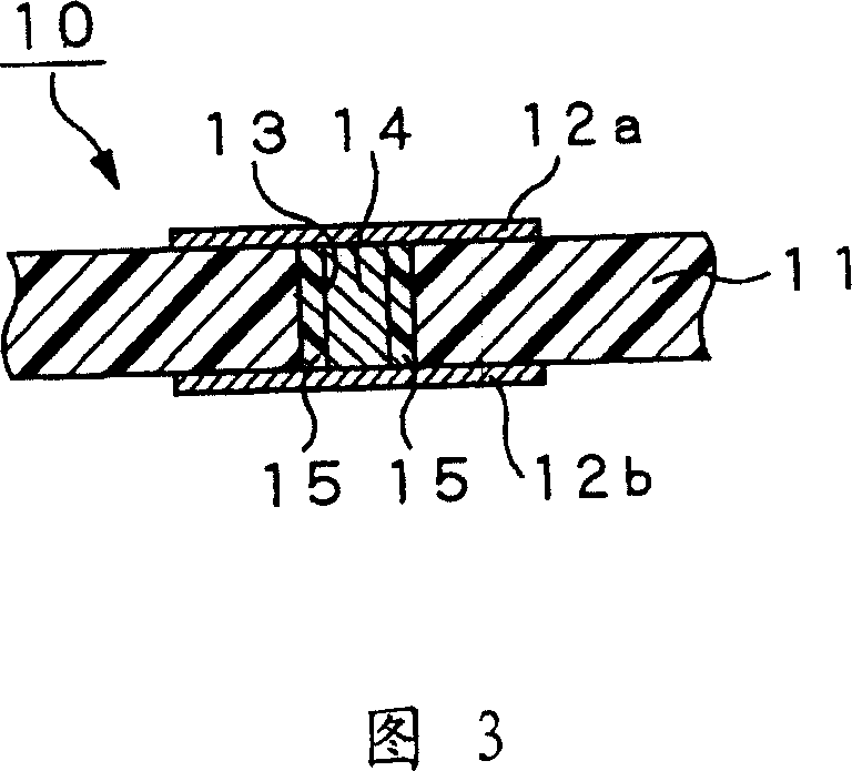
[0036] As shown in FIG. 3 , the multilayer wiring board 10 includes a base material 11 and metal conductor patterns 12 ( 12 a , 12 b ) formed on both sides (upper and lower surfaces) of the base material 11 . Through holes 13 penetrating the lower surface of the base material 11 from the upper surface thereof are formed in the base material 11 . The interlayer connection member 14 is formed in the through hole 13 . The upper and lower openings of the through holes 13 are covered with the conductor patterns 12 (12a, 12b). The interlayer connection members 14 are connected to the conductor patterns 12 (12a, 12b) formed on both sides of the base material...


PUM


Abstract

The invention improves reliability of interlayer connection of a multilayer wiring board. Plural metal conductor pattern layers are formed on a base material made of thermoplastic resin. Then, high melting metal containing copper, low melting metal containing tin, and binder resin are packed into a via hole. Subsequently, predetermined heat and pressure are applied. Then, while half-melted metal mixture droplets of the low and high melting metals and melted binder resin are phase separated from each other, the surfaces of the conductor patterns that face the openings of the via and the low melting metal are alloyed with each other to form an alloy layer as well as the high and low meting metals are alloyed with each other to form a columnar-shaped interlayer connection part. As a result, an intermediate layer is formed between the outer surface of the columnar-shaped interlayer connection part and inner surface of the via hole.

Description

technical field [0001] The present invention relates to a multilayer wiring board in which a plurality of metal conductor pattern layers are formed on a base material made of thermoplastic resin and a manufacturing method thereof. Background technique [0002] With the widespread use of portable electronic devices such as mobile phones, digital still cameras, etc., build-up boards have entered the forefront of the market. Integrated boards are used to achieve ultra-miniaturization of components and fine patterns or miniaturization of through-hole sizes for high-density devices. However, integrated boards are produced based on a so-called sequential multilayer wiring technique in which individual layers are sequentially formed and laminated, complicating the board production process. [0003] In these cases, methods once applied to ceramic multilayer boards using unfired sheets are now being applied to organic materials as well. In this method, vias, wiring patterns, etc. f...

Claims


Application Information

Patent Timeline
IPC IPC(8): H05K1/09H05K1/11H05K1/00H05K3/46
Inventor 中田昌和小川稔
Owner SONY CORP
Why Eureka
Try Eureka