

Method for realizing general digital quantity regulation
A realization method and a technology of signal conditioning, applied in the direction of electrical digital data processing, instruments, calculations, etc., can solve the problems of bulky, time-consuming, laborious, uneconomical, etc., and achieve the effect of low material cost, wide adaptability, and simple operation
- Summary
- Abstract
- Description
- Claims
- Application Information
AI Technical Summary
Problems solved by technology
Method used
Image

Examples
Embodiment Construction
[0015] 1. The method for realizing general conditioning of digital output signals comprises the following steps:
[0016] 1. Circuit structure
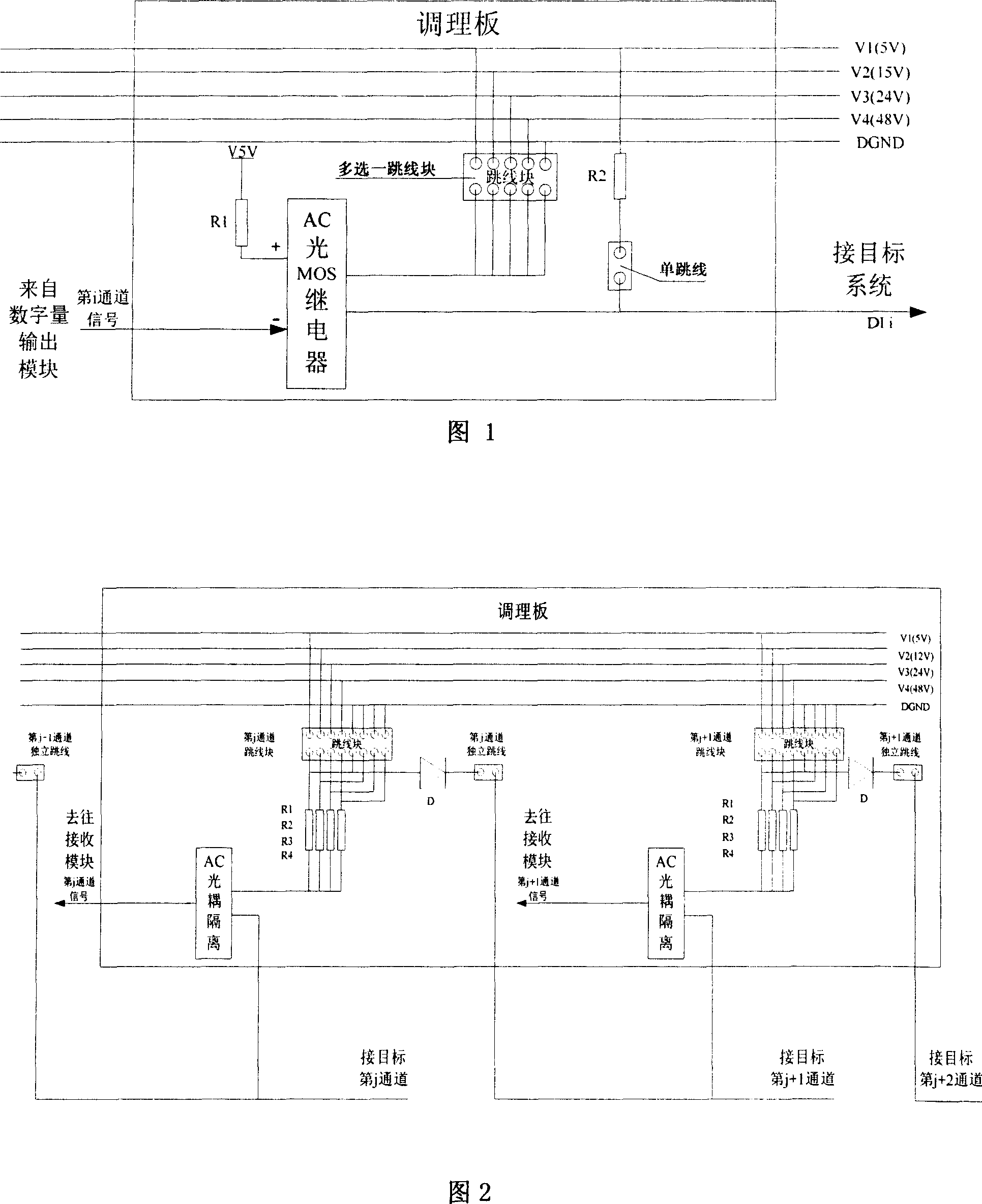
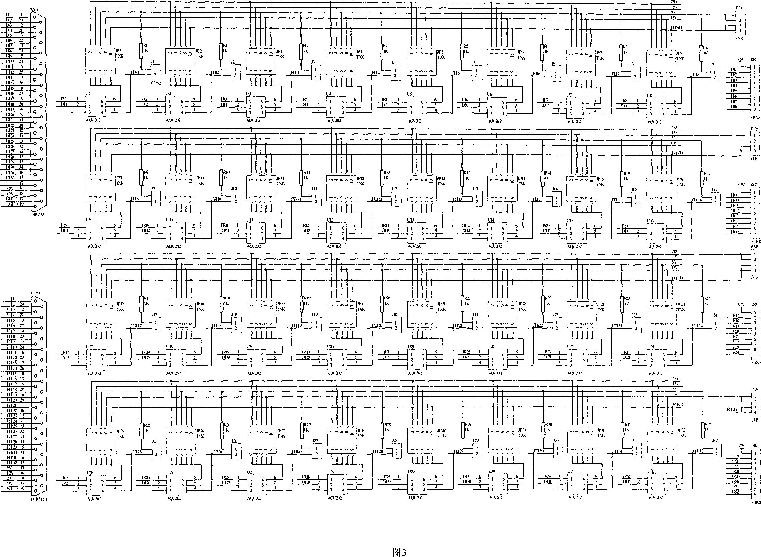
[0017] Its circuit diagram is shown in Fig. 1. According to the analysis of various types of digital output signals, combined with the development of device technology, the digital output signal conditioning circuit of the present invention consists of the following parts:
[0018] A bidirectional optical control isolation MOS relay is set on the conditioning board, and the output signal from the control system is isolated from the output signal of the conditioning circuit through the bidirectional optical control isolation MOS relay. The positive input terminal (+) of the bidirectional optical control isolation MOS relay There is a resistor R1 connected to the 5V power supply of the input signal, and the negative input terminal (-) of the bidirectional optical control isolation MOS relay is connected to the TTL signal output from th...
PUM
 Abstract
Description
Claims
Application Information