Semiconductor device and method for manufacturing the same

A manufacturing method and semiconductor technology, applied in the direction of semiconductor/solid-state device manufacturing, semiconductor devices, electric solid-state devices, etc., can solve the problems of reduced protection performance, reduced controllability of plasma damage, difficulty in efficiently releasing plasma current, etc., to prevent Plasma current destruction, the effect of avoiding the rise of withstand voltage

Inactive Publication Date: 2007-04-11
LAPIS SEMICON CO LTD
View PDF0 Cites 2 Cited by
  • Summary
  • Abstract
  • Description
  • Claims
  • Application Information

AI Technical Summary

Problems solved by technology

Therefore, there is a problem that it is difficult to efficiently discharge surge currents such as plasma currents, and the protection performance is reduced.
In addition, if the withstand voltage of the diode is increased in this way, there is also a problem that the controllability of the plasma damage is lowered.

Method used


Image

  • Semiconductor device and method for manufacturing the same
  • Semiconductor device and method for manufacturing the same
  • Semiconductor device and method for manufacturing the same

Examples


Embodiment 1

[0038] First, Embodiment 1 of the present invention will be described in detail with reference to the drawings. Furthermore, in this embodiment, the semiconductor element formed on the SOI substrate is used as an inverter as an example for description.

[0039] · Overall composition

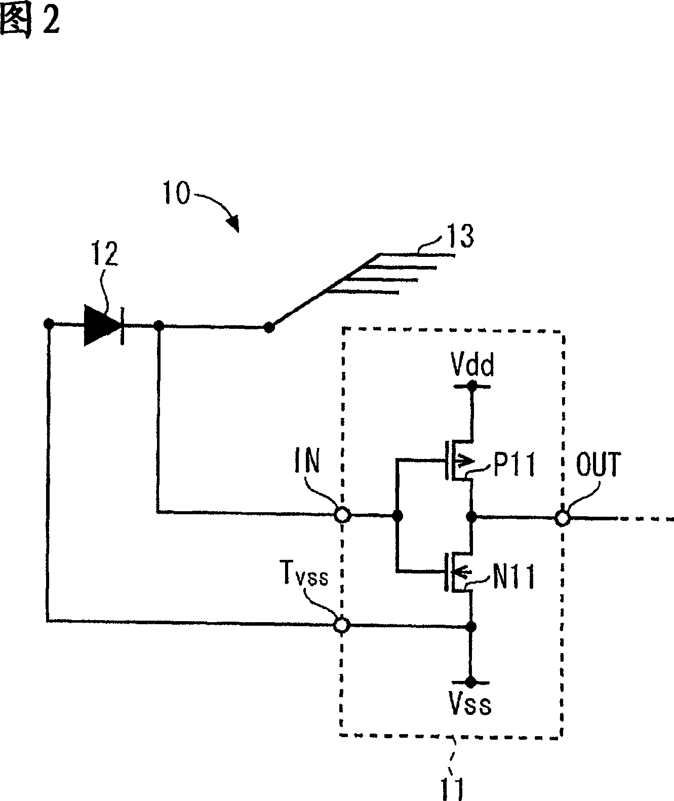
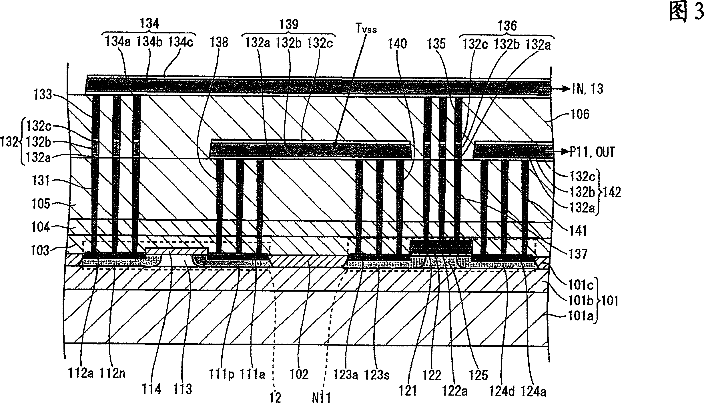
[0040]FIG. 2 is a circuit diagram showing the configuration of the semiconductor device 10 of the present embodiment. As shown in FIG. 2 , the semiconductor device 10 has a PMOS transistor P11 and an NMOS transistor N11 connected in series between a power supply line Vdd and a power supply line Vss. The drains of the PMOS transistor P11 and the NMOS transistor N11 are connected in common and connected to the output terminal OUT. The source of the PMOS transistor P11 is connected to the power supply line Vdd. The source of the NMOS transistor N11 is connected to the power supply line Vss and also connected to the Vss terminal Tvss (second terminal). The gates of the PMOS transistor P11 and the...

Embodiment 2

[0090] Next, Embodiment 2 of the present invention will be described in detail with reference to the drawings. In addition, in the following description, the same code|symbol is attached|subjected to the same structure as Example 1, and the detailed description is abbreviate|omitted. In addition, about the structure which is not specifically described, it is the same as Example 1. In addition, in this embodiment, as in the first embodiment, a semiconductor element formed on an SOI substrate is used as an example for an inverter.

[0091] · Overall composition

[0092] FIG. 10 is a circuit diagram showing the configuration of the semiconductor device 20 of this embodiment. As shown in FIG. 10 , the semiconductor device 20 has the same configuration as the semiconductor device 10 of the first embodiment (see FIG. 2 ), and has a structure in which a wiring connecting the anode of the protection diode 12 and the Vss terminal Tvss is connected to the substrate. . Note that othe...


PUM


Abstract

Provided is a semiconductor device which can be prevented from breaking by plasma current in a manufacturing process, and keep a breakdown voltage of diode from rising simultaneously; and to provide a manufacturing method of the semiconductor device. A semiconductor device 10 comprises an SOI substrate 101 having a silicon substrate 101a a supporting substrate, an oxide film 101b on the silicon substrate 101a, and a silicon thin film 101c on the oxide film 101b; an input terminal IN (a second upper layer interconnect line 134) formed on the silicon thin film 101c; a Vss terminal Tvss (a first upper layer interconnect line 139) formed on the silicon thin film 101c; a semiconductor device formed on the silicon thin film 101c, which is connected to the input terminal IN and Vssterminal Tvss (e.g. the inverter 11); and a protection diode 12, formed on the silicon thin film 101c, which is connected in a forward direction from the Vss terminal Tvss to the input terminal IN.

Description

technical field [0001] The present invention relates to a semiconductor device and a method for manufacturing the semiconductor device, in particular to a semiconductor device using an SOI substrate and a method for manufacturing the semiconductor device, and also for preventing damage in the manufacturing process and a method for manufacturing the semiconductor device. Background technique [0002] Conventionally, in a semiconductor device using a bulk substrate, a protection diode is forwardly connected between the input terminal of the circuit and the substrate in order to prevent damage to the semiconductor element due to plasma current during the manufacturing process. The circuit configuration of a semiconductor device 90 having such a configuration is shown in FIG. 1 . In addition, in this description, the semiconductor device 90 in which the inverter 91 is incorporated in a bulk substrate is taken as an example. [0003] As shown in FIG. 1, a semiconductor device 90...

Claims


Application Information

Patent Timeline
Patent Type & Authority Applications(China)
IPC IPC(8): H01L27/12H01L21/84
CPCH01L29/41733H01L27/1203H01L27/0251H01L29/665H01L21/20H01L27/12
Inventor 袋武人冲原将生
Owner LAPIS SEMICON CO LTD
Why Eureka
Try Eureka