Light emitting device using electron emission and flat display apparatus using the same

A flat-panel display device and light-emitting device technology, applied in the direction of electric solid-state devices, discharge tube/lamp parts, electric light sources, etc., can solve the problems of repeatability and reliability

Inactive Publication Date: 2007-04-18
SAMSUNG SDI CO LTD
View PDF2 Cites 3 Cited by
  • Summary
  • Abstract
  • Description
  • Claims
  • Application Information

AI Technical Summary

Problems solved by technology

However, traditional methods of forming nanometer-sized gaps have had some problems with repeatability and / or reliability

Method used


Image

  • Light emitting device using electron emission and flat display apparatus using the same
  • Light emitting device using electron emission and flat display apparatus using the same
  • Light emitting device using electron emission and flat display apparatus using the same

Examples


Embodiment Construction

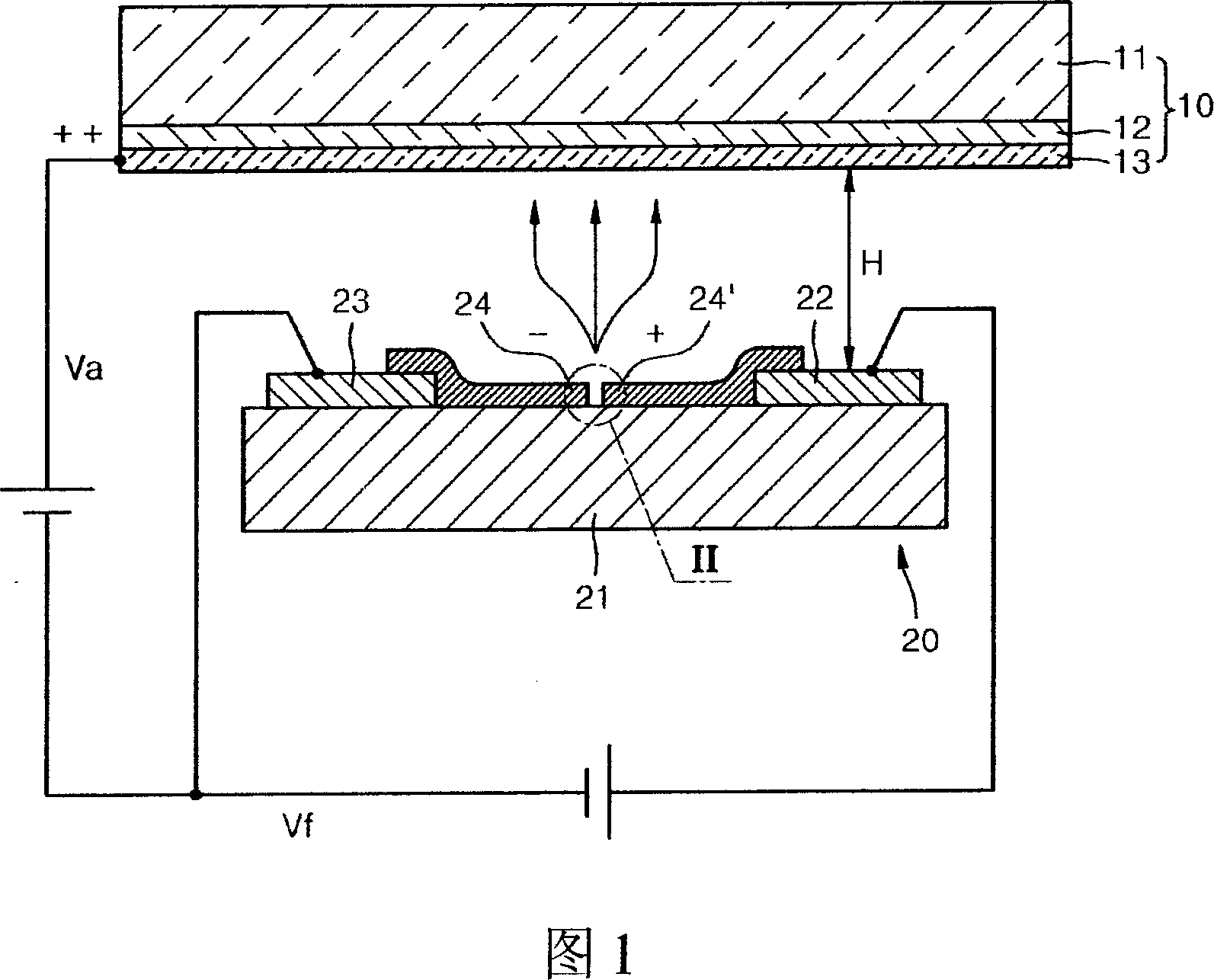
[0030] Embodiments of the present invention provide a light emitting device using electron emission having low driving voltage and high luminous efficiency, and a flat panel display device using the light emitting device.

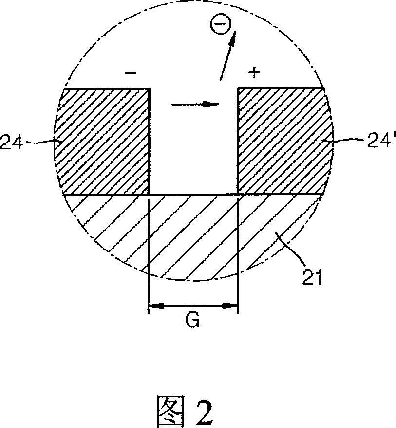
[0031] Embodiments of the present invention also provide a light emitting device using electron emission having nanometer-sized gaps that can be formed repeatedly and with reliability.

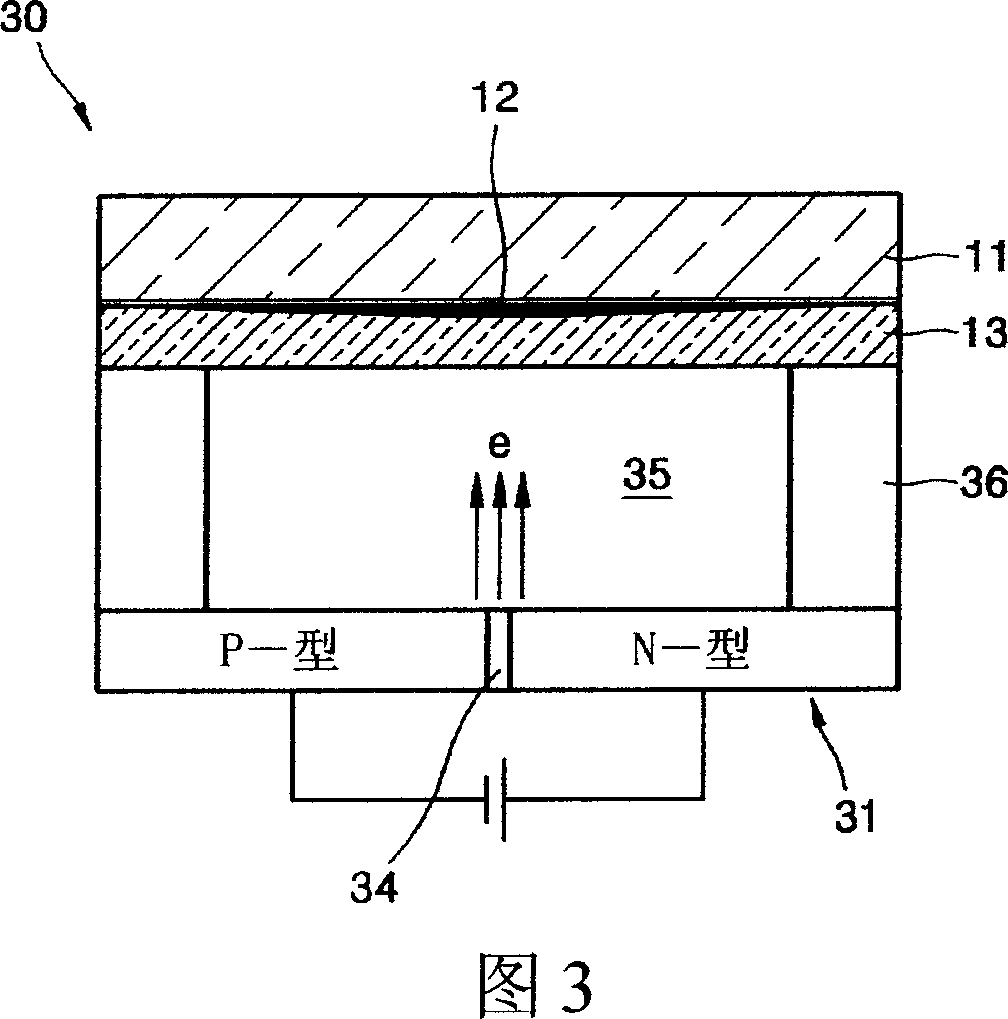
[0032] FIG. 3 is a schematic cross-sectional view of a light emitting device 30 using electron emission according to the first embodiment. FIG. 4 is a graph illustrating current characteristics of the PN junction 31 used in the light emitting device 30 shown in FIG. 3 .

[0033] Referring to FIG. 3 , the light emitting device 30 includes a PN junction 31 , an anode 12 and a phosphor layer 13 .

[0034] In a region where the p-type semiconductor and the n-type semiconductor are combined, the PN junction 31 includes a depletion layer 34 having a predetermined thickness. The a...


PUM

PropertyMeasurementUnit
thicknessaaaaaaaaaa

Abstract

Provided are a light emitting device using electron emission with a low driving voltage and high luminous efficiency, and a flat display apparatus using the light emitting device. In addition, a light emitting device using electron emission in which with a nano-sized gap can be formed with repeatability and have reliability is provided. The light emitting device includes: a plurality of PN junctions (34), each including a depletion layer having a predetermined thickness; an anode electrode (12) facing the depletion layer and separated from the depletion layer by a predetermined distance; and a phosphor layer (13) formed on a surface of the anode electrode. The flat display apparatus includes the light emitting device.

Description

[0001] Cross references to patent applications [0002] This application claims the benefit of Korean Patent Application No. 10-2005-0095487 filed with the Korean Intellectual Property Office on Oct. 11, 2005, which is incorporated herein by reference. technical field [0003] Embodiments of the present invention relate to a light emitting device using electron emission and a flat panel display device using the light emitting device, and more particularly to a light emitting device using electron emission having a low driving voltage and high luminous efficiency, and a light emitting device using the light emitting device Flat panel display device. Background technique [0004] A plasma display panel (PDP), which is a flat panel display device, uses electric discharge to form images. DPD is widely used due to its outstanding display characteristics such as high brightness and large viewing angle. PDPs can be classified into a facing discharge type or a surface discharge ty...

Claims


Application Information

Patent Timeline
Patent Type & Authority Applications(China)
IPC IPC(8): H01J1/308H01J17/04H01J29/04C09K11/08C09K11/77H01J17/20H01J17/49H01J31/12G09F9/30H01L33/00H01L27/15F21S2/00F21Y101/00F21Y105/00G02F1/13357H01J63/06H01J63/08
CPCH01J31/127G02F1/133602H01J1/308H01J63/02G02F2001/133625H01J29/481H01J63/08G02F1/133625H01J1/63
Inventor 孙承贤金起永
Owner SAMSUNG SDI CO LTD
Why Eureka
Try Eureka