
Method and device for testing oxide of grid electrode by using fuse wire

A fuse and bias technology, applied in the direction of measuring devices, measuring electricity, measuring electrical variables, etc., to achieve rapid detection, improve detection reliability, and improve detection sensitivity

Inactive Publication Date: 2007-05-09
SEMICON MFG INT (SHANGHAI) CORP +1
View PDF0 Cites 3 Cited by
  • Summary
  • Abstract
  • Description
  • Claims
  • Application Information

AI Technical Summary

Problems solved by technology

However, such existing methods and devices for breakdown detection have limited reliability and sensitivity

Method used


Image

  • Method and device for testing oxide of grid electrode by using fuse wire
  • Method and device for testing oxide of grid electrode by using fuse wire
  • Method and device for testing oxide of grid electrode by using fuse wire

Examples


Embodiment Construction

[0016] The present invention relates generally to integrated circuits. More specifically, the present invention provides a method and apparatus for testing an oxide layer using a fuse. Merely by way of example, the invention has been applied to testing gate oxide layers. It should be recognized, however, that the invention has broader applicability.

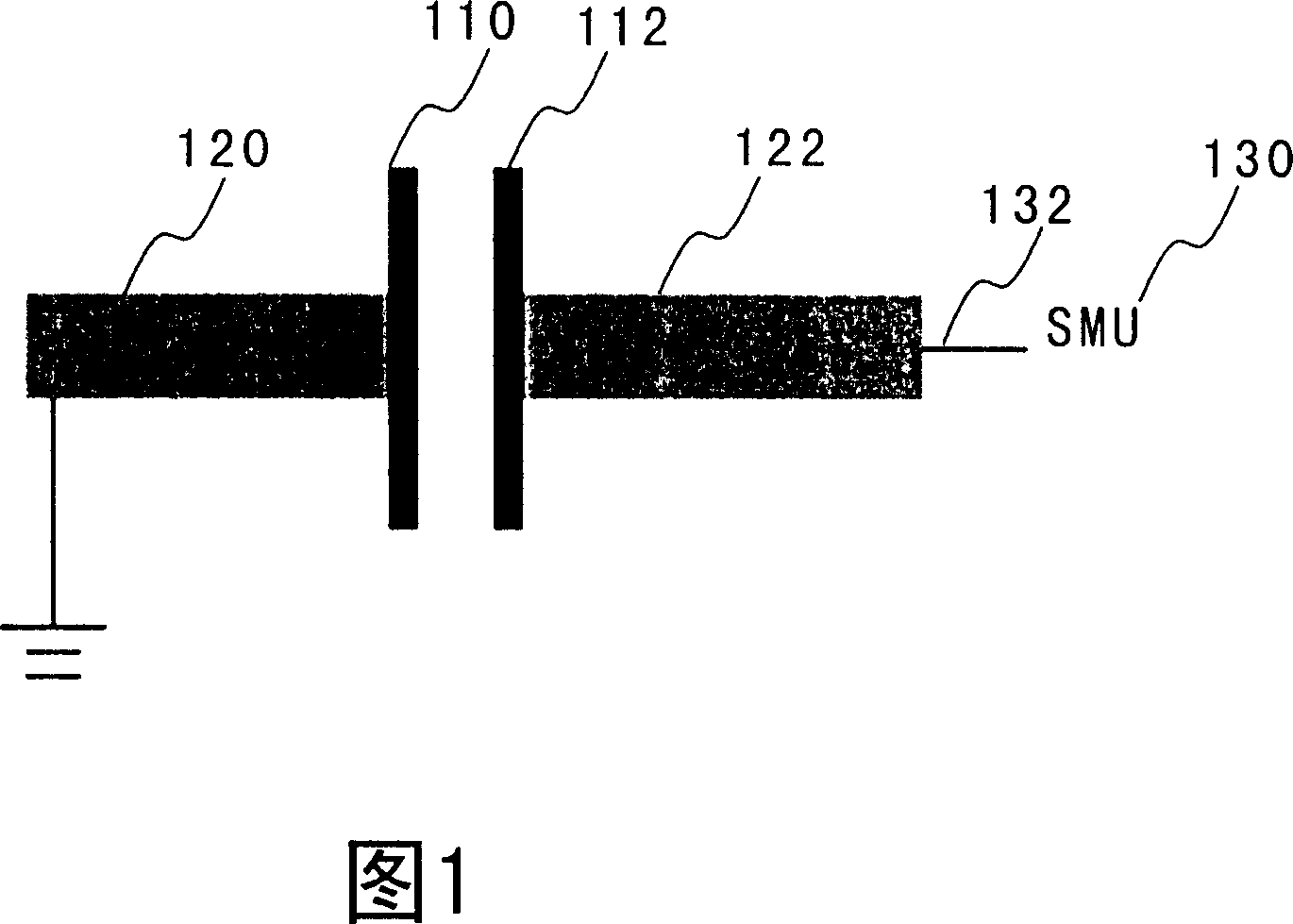
[0017] As mentioned above, in FIG. 1, when the gate oxide layer breaks down, the current flowing through the wire 122 will become very high. High currents can burn the metal wires 122 and / or damage the probe card 132 . If the metal wire 122 is burned out, the metal wire 122 is disconnected, and the current flowing through the metal wire decreases rapidly. Therefore, breakdown of the gate oxide layer can become difficult to detect.

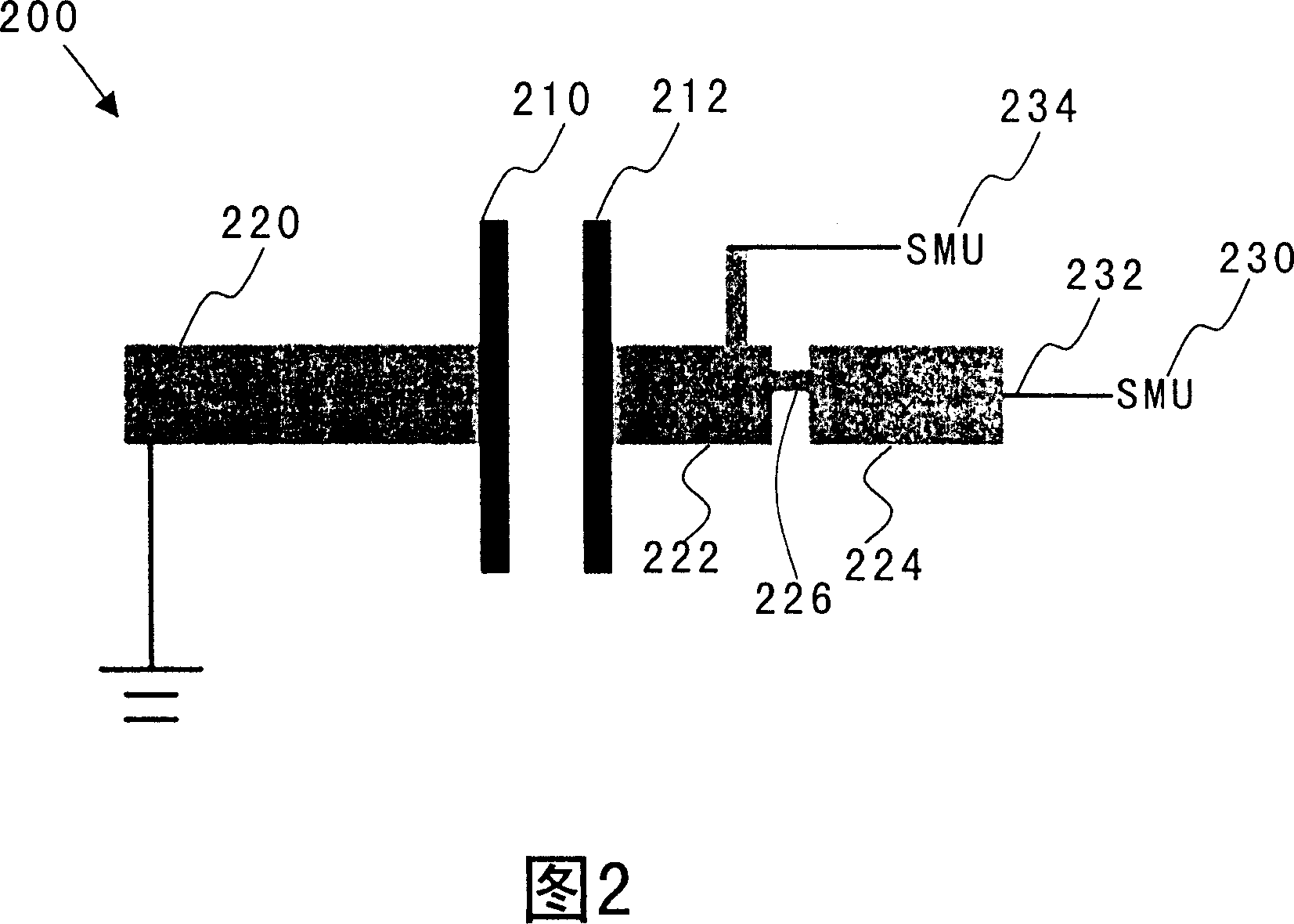
[0018] FIG. 2 is a simplified setup for testing a gate oxide layer according to an embodiment of the present invention. This diagram is merely an example, which should not unduly limit the scope ...


PUM


Abstract

A device using fuse to test oxide of grid is prepared as directly contacting the first and the second conduction plates to electric media layer, connecting the first conduction wire to the first conduction plate and biasing said wire to the first preset voltage, connecting the second conduction wire to the second conduction plate and voltage detector, connecting fuse to the second conduction wire and connecting the third conduction wire to fuse and component enabling to provide the second preset voltage and enabling to measure current.

Description

technical field [0001] The present invention relates generally to integrated circuits. More specifically, the present invention provides a method and apparatus for testing an oxide layer using a fuse. Merely by way of example, the invention has been applied to testing gate oxide layers. It should be recognized, however, that the invention has broader applicability. Background technique [0002] Integrated circuits, or "ICs," have grown from a handful of interconnected devices fabricated on a single silicon chip to millions of devices. Current integrated circuits offer performance and complexity far beyond what was originally envisioned. In order to achieve progress in complexity and circuit density (i.e., the number of devices that can be packaged on a given chip area), the minimum device feature size (also known as device "geometry") accompanies the development of each generation of integrated circuits and become smaller. Semiconductor devices are now being fabricated ...

Claims


Application Information

Patent Timeline
Patent Type & Authority Applications(China)
IPC IPC(8): G01N27/92G01R31/00
CPCG01R31/2856G01R31/2831
Inventor 龚斌
Owner SEMICON MFG INT (SHANGHAI) CORP
Learn More