Method for manufacturing plasma display panel
A technology for display panels and manufacturing methods, applied in the manufacture of ships or lead-in wires, manufacturing tools, glass manufacturing equipment, etc., can solve the problems of damage to the unit panel discharge field and the inability to uniformly cut unit panels, etc., to reduce the defective rate, The effect of increasing production yield
- Summary
- Abstract
- Description
- Claims
- Application Information
AI Technical Summary
Problems solved by technology
Method used
Image

Examples
Embodiment Construction
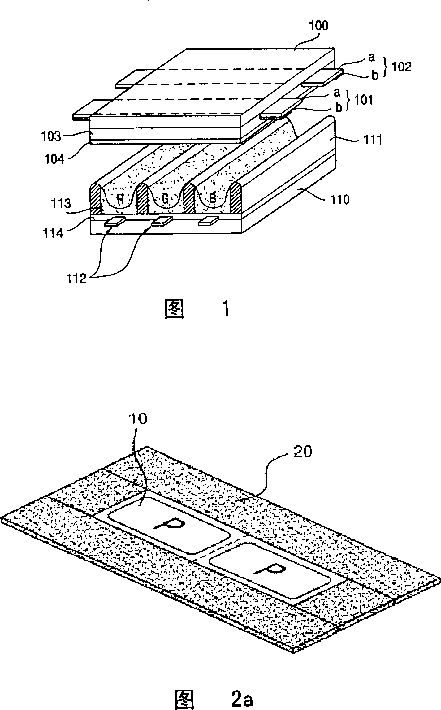
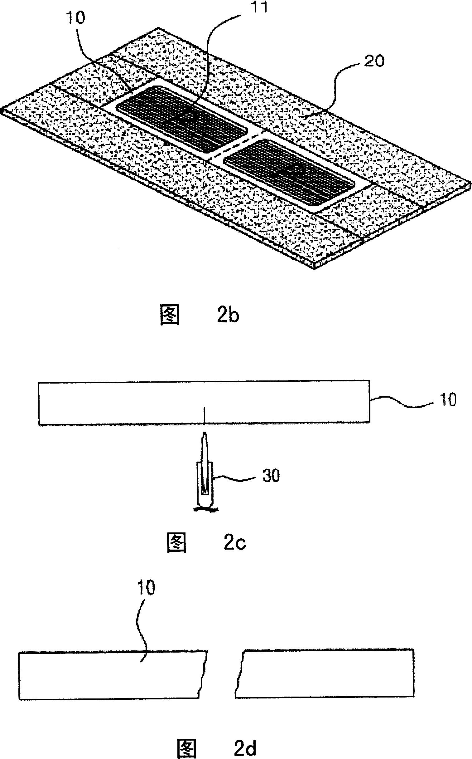
[0027] Hereinafter, embodiments of a method of manufacturing a plasma display panel of the present invention will be described in detail with reference to the accompanying drawings.
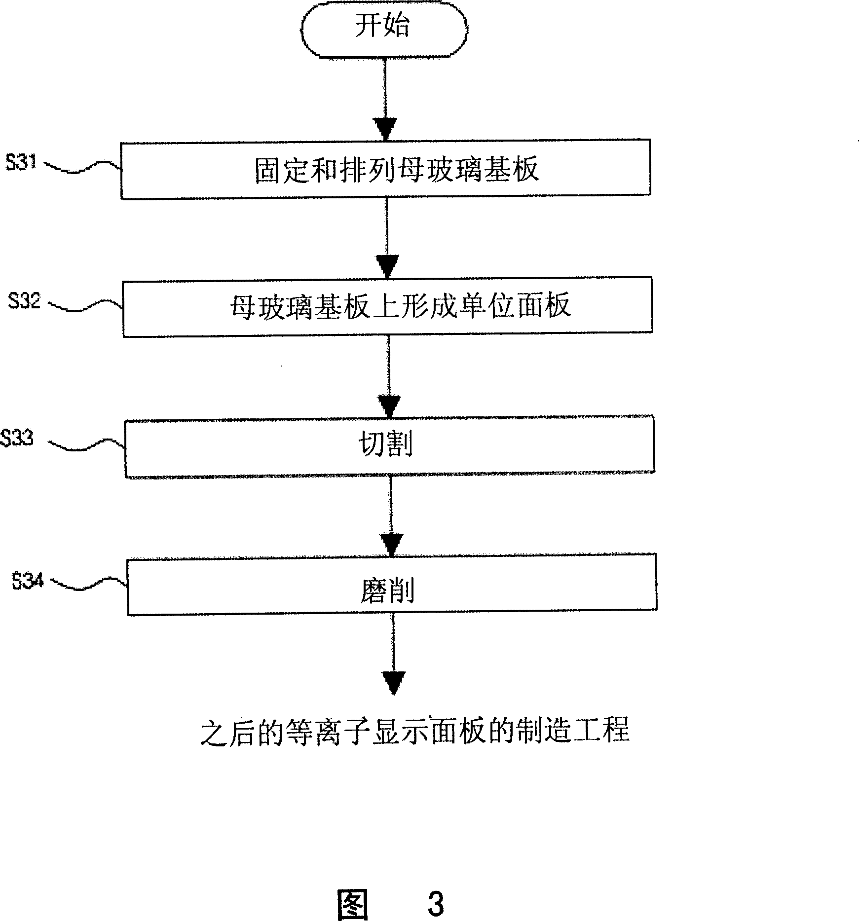
[0028] FIG. 3 is a schematic view showing the multi-facet acquisition process sequence in the method of manufacturing the plasma display panel of the present invention.
[0029] FIG. 3 is a process diagram showing the process sequence of multi-face acquisition in the method of manufacturing the plasma display panel of the present invention.
[0030] As shown in Figure 4:
[0031] S31, the multi-faceted process of the plasma display panel of the present invention includes the stage of fixing and arranging the mother glass substrate with the guide metal plate.
[0032] S32, after fixing and arranging the mother glass substrate, forming several unit panels on the mother glass substrate.
[0033] S33, S34, after forming the above-mentioned unit panel, when cutting (Cuttint) along the cut surface of...
PUM
 Abstract
Description
Claims
Application Information
 - R&D
- Intellectual Property
- Life Sciences
- Materials
- Tech Scout
- Unparalleled Data Quality
- Higher Quality Content
- 60% Fewer Hallucinations
Browse by: Latest US Patents, China's latest patents, Technical Efficacy Thesaurus, Application Domain, Technology Topic, Popular Technical Reports.
© 2025 PatSnap. All rights reserved.Legal|Privacy policy|Modern Slavery Act Transparency Statement|Sitemap|About US| Contact US: help@patsnap.com