Transimpedance amplifier

A technology of transconductance amplifier and amplifying circuit, applied in the field of transconductance amplifier, can solve the problems of reducing transconductance gain, waveform distortion, small distortion, etc.

Active Publication Date: 2007-07-04
NIPPON TELEGRAPH & TELEPHONE CORP +1
View PDF1 Cites 17 Cited by
  • Summary
  • Abstract
  • Description
  • Claims
  • Application Information

AI Technical Summary

Problems solved by technology

[0004] In this type of transconductance amplifier, as the input current Iin increases, the amplitude of the output voltage Vout saturates, resulting in waveform distortion
Therefore, in order to meet the requirements of both high sensitivity and wide dynamic range characteristics, by re...

Method used


Image

  • Transimpedance amplifier
  • Transimpedance amplifier
  • Transimpedance amplifier

Examples


no. 1 example

[0118] The configuration of a transconductance amplifier according to a first embodiment of the present invention will be described with reference to FIGS. 1 and 2 .

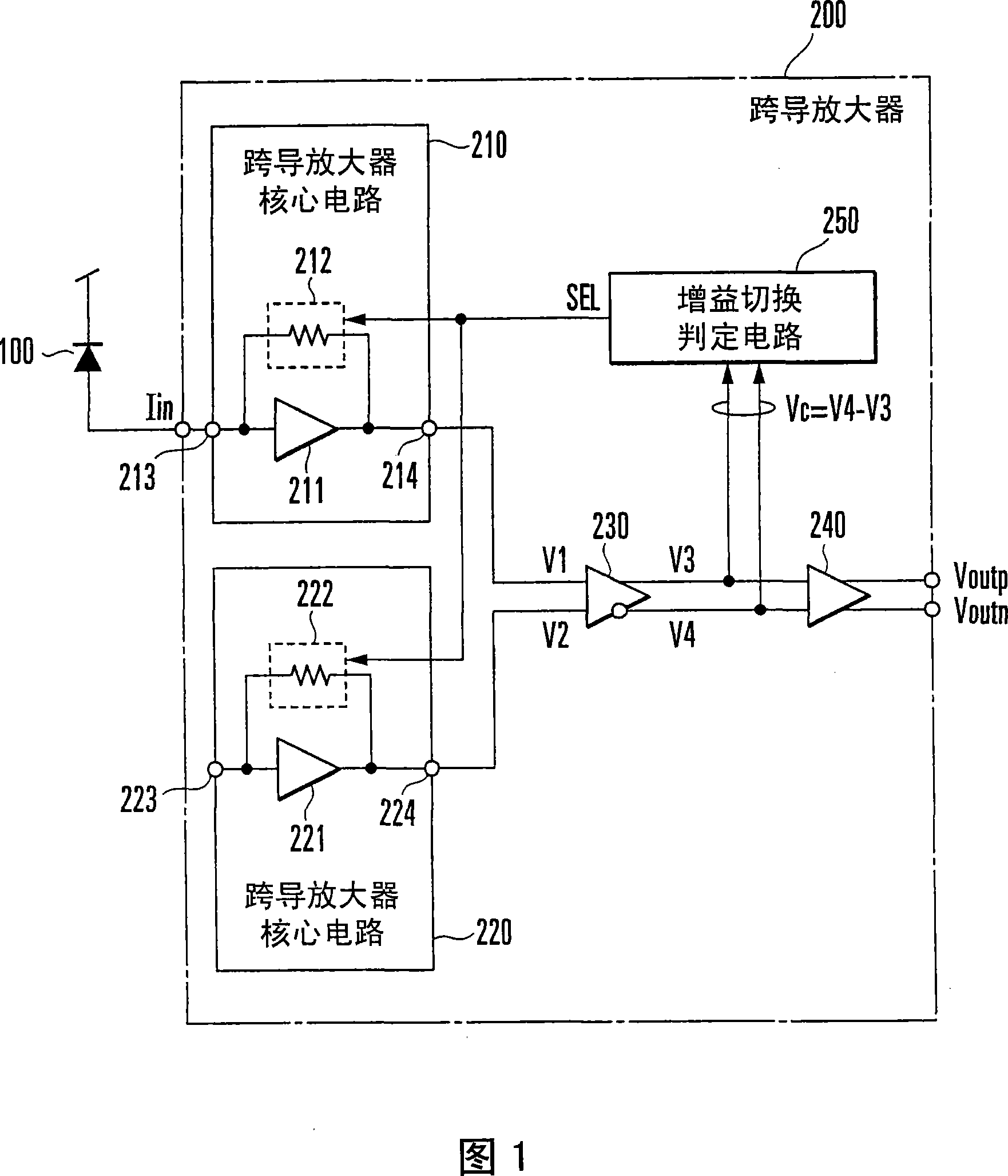
[0119] In an optical transmission circuit such as an optical transmission system, an optical interconnection, or a passive optical network (OPN) system capable of performing high-speed data transmission, an optical signal that is received by the light receiving element 100 and transmitted through an optical fiber is converted into an electrical signal. The receiving circuit adopts the transconductance amplifier 200 shown in FIG. 1 .

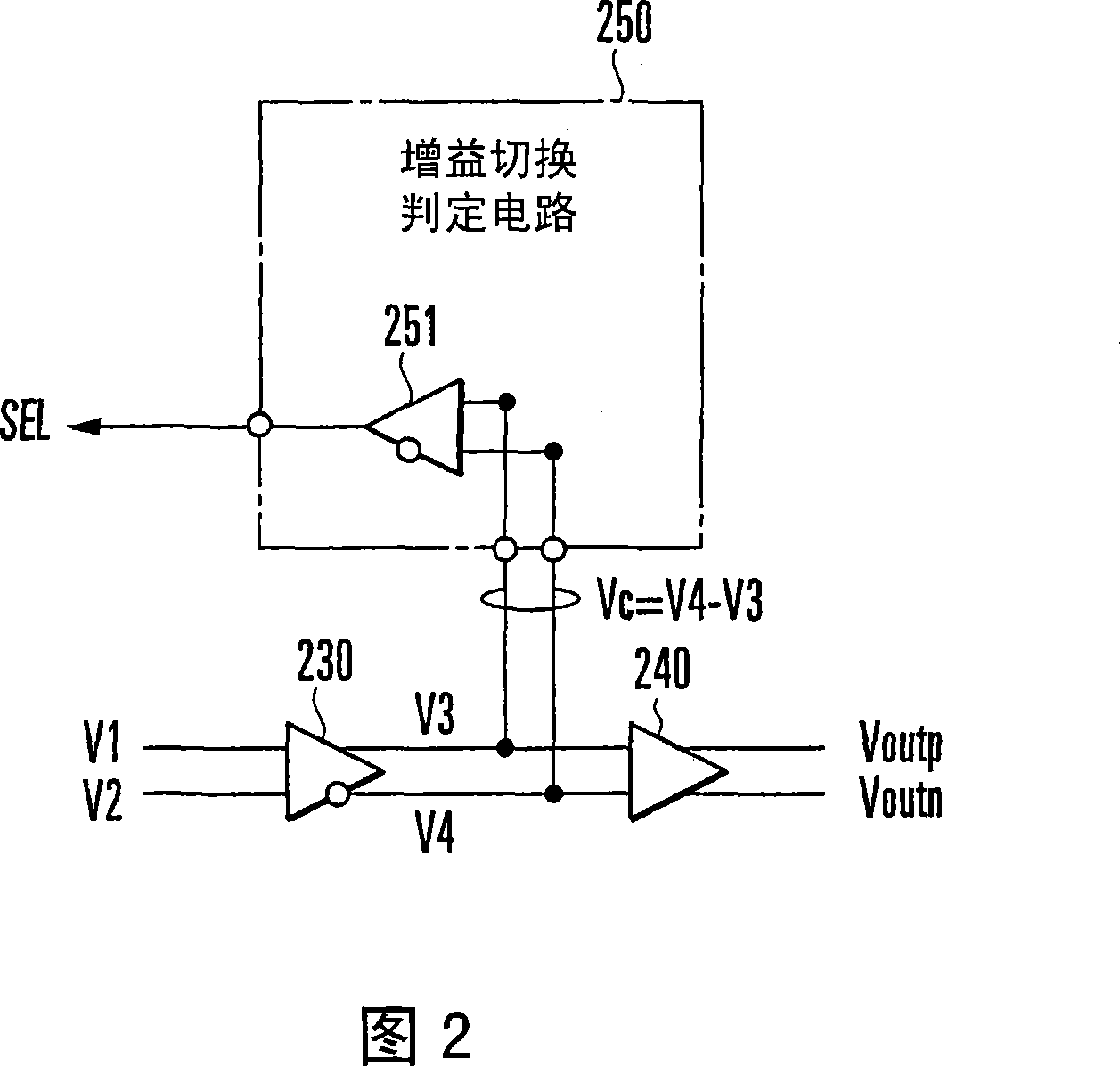
[0120] As shown in FIG. 1 , the transconductance amplifier 200 mainly includes a first transconductance amplifier core circuit 210 , a second transconductance amplifier core circuit 220 , an interstage buffer circuit 230 , an output buffer circuit 240 and a gain switching determination circuit 250 .

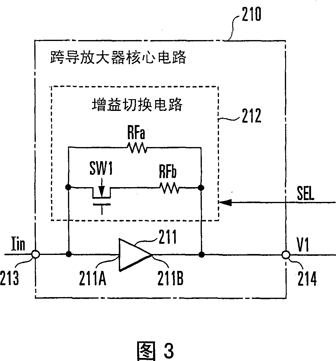
[0121] The first transconductance amplifier core circuit 210 includes an amplific...

no. 2 example

[0156] Next, the configuration of a transconductance amplifier according to a second embodiment of the present invention will be described with reference to FIGS. 9 to 11 . In FIGS. 9 to 11, the same reference numerals as in FIGS. 2 to 4 denote the same components.

[0157] The case of switching the gain of the core circuits 210 and 220 of the transconductance amplifier between "high gain" and "low gain" by one step has been exemplified in the first embodiment. The second embodiment will exemplify the case of switching the gain through multiple steps, specifically, switching the core circuit 210 of the transconductance amplifier between "high gain", "intermediate gain" and "low gain" through two steps and a gain of 220 in the case. Note that the constituent elements of the transconductance amplifier according to this embodiment are the same as those in the first embodiment except for the gain switching determination circuit and the first and second transconductance amplifier ...

no. 3 example

[0177] Next, a transconductance amplifier core circuit employed in a transconductance amplifier according to a third embodiment of the present invention will be described with reference to FIGS. 14 to 16 .

[0178] Each of the transconductance amplifier core circuits 210B and 220B in FIG. 14 includes a transconductance gain switching circuit 281 for switching the transconductance gain and an open-loop gain switching circuit 282, which communicates with the "high gain" in two steps. Each of the gain switching circuits 212B and 222B that switch the gain between , "middle gain" and "low gain" switches the open-loop gain in the same manner.

[0179] The transconductance gain switching circuit 281 includes feedback resistors RF1, RF2, and RF3 that determine the transconductance gain, and NMOS transistors MN1 and MN2 that operate as switches. The open-loop gain switching circuit 282 includes load resistors RL1, RL2, and RL3 that determine an open-loop gain, and NMOS transistors MN3 ...


PUM


Abstract

A gain switch determination circuit (250) uses a first hysteresis characteristic to perform a comparison/determination of a comparison input voltage (Vc) from an inter-stage buffer circuit (230), and a gain switch signal (SEL) based on a result of the comparison/determination is outputted to first and second transimpedance amplifier core circuits (210,220), thereby switching the gains of those core circuits. This eliminates the necessity of using a level hold circuit, which exhibits a slow response, to hold the comparison input voltage so as to perform a gain switch determination. As a result, an instant gain switch determination can be achieved, thereby realizing an instant response to burst data.

Description

technical field [0001] The present invention relates to a transconductance amplifier, which receives a current signal obtained by photoelectric conversion using a light receiving element, and converts / amplifies the signal into a voltage signal in a light receiving circuit. Specifically, the present invention relates to a Transconductance amplifiers that can handle input currents with a large dynamic range. Background technique [0002] In optical transmission circuits that can perform high-speed data transmission, such as optical transmission systems, optical interconnections, and passive optical network (hereinafter referred to as PON (passive optical network)) systems, the optical receiving circuit that converts optical signals into electrical signals uses transconductance amplifier. [0003] The transconductance amplifier receives the input current Iin obtained by photoelectrically converting the received optical signal using a light receiving element, converts the curre...

Claims


Application Information

Patent Timeline
IPC IPC(8): H03G3/30H04B10/14H03G3/20H04B10/26H03F3/08H04B10/28H04B10/06H04B10/43
Inventor 中村诚楳田洋太郎远藤润赤津祐史今井祐记十林正俊卜部义和饭塚初史兵头荣治
Owner NIPPON TELEGRAPH & TELEPHONE CORP
Why Eureka
Try Eureka