

Lithographic apparatus and device manufacturing method
A technology of equipment and lithography projection, which is applied in micro-lithography exposure equipment, semiconductor/solid-state device manufacturing, optomechanical equipment, etc., can solve the problem of insignificant error and so on
- Summary
- Abstract
- Description
- Claims
- Application Information
AI Technical Summary
Problems solved by technology
Method used
Image

Examples
Embodiment Construction
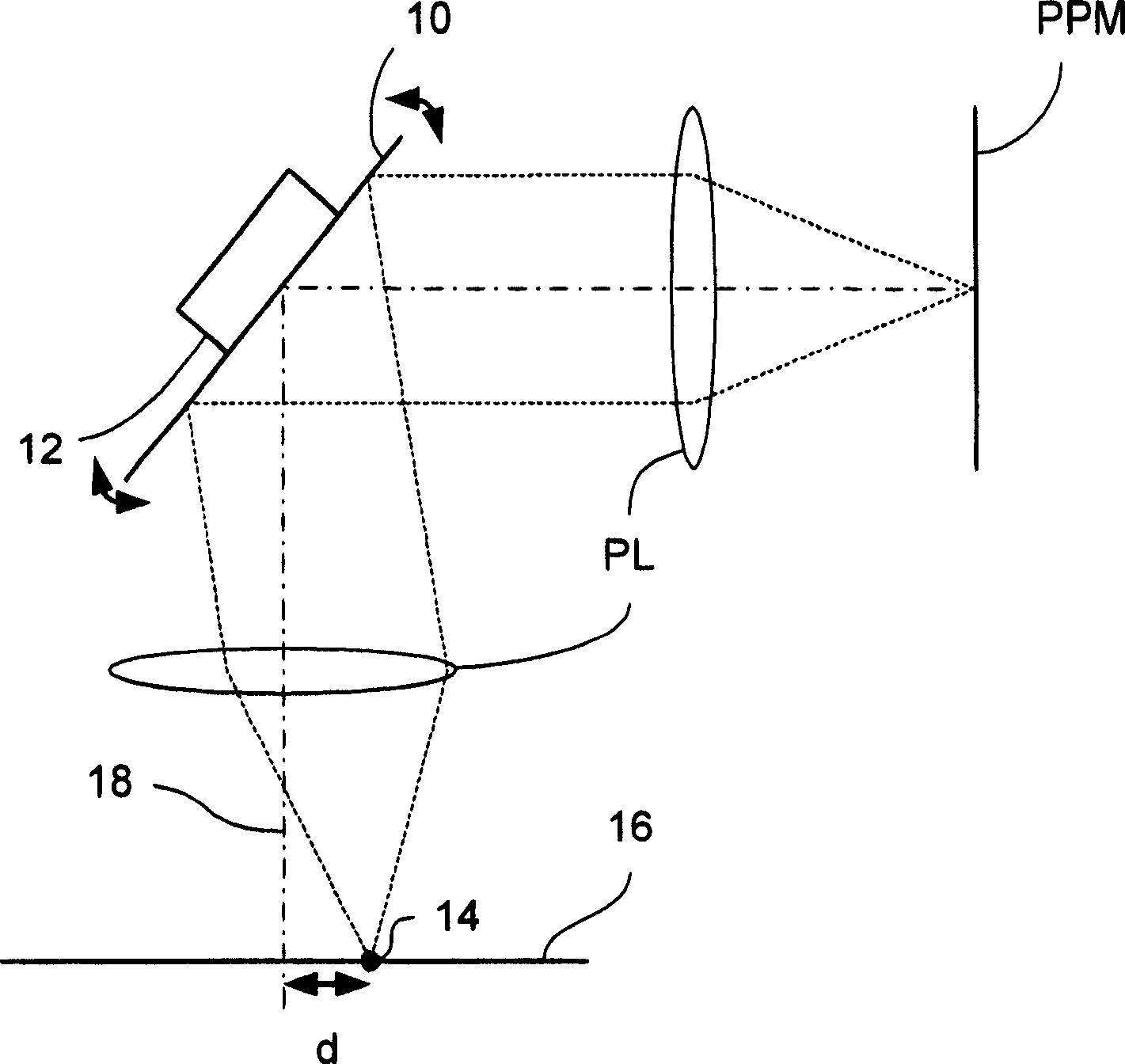
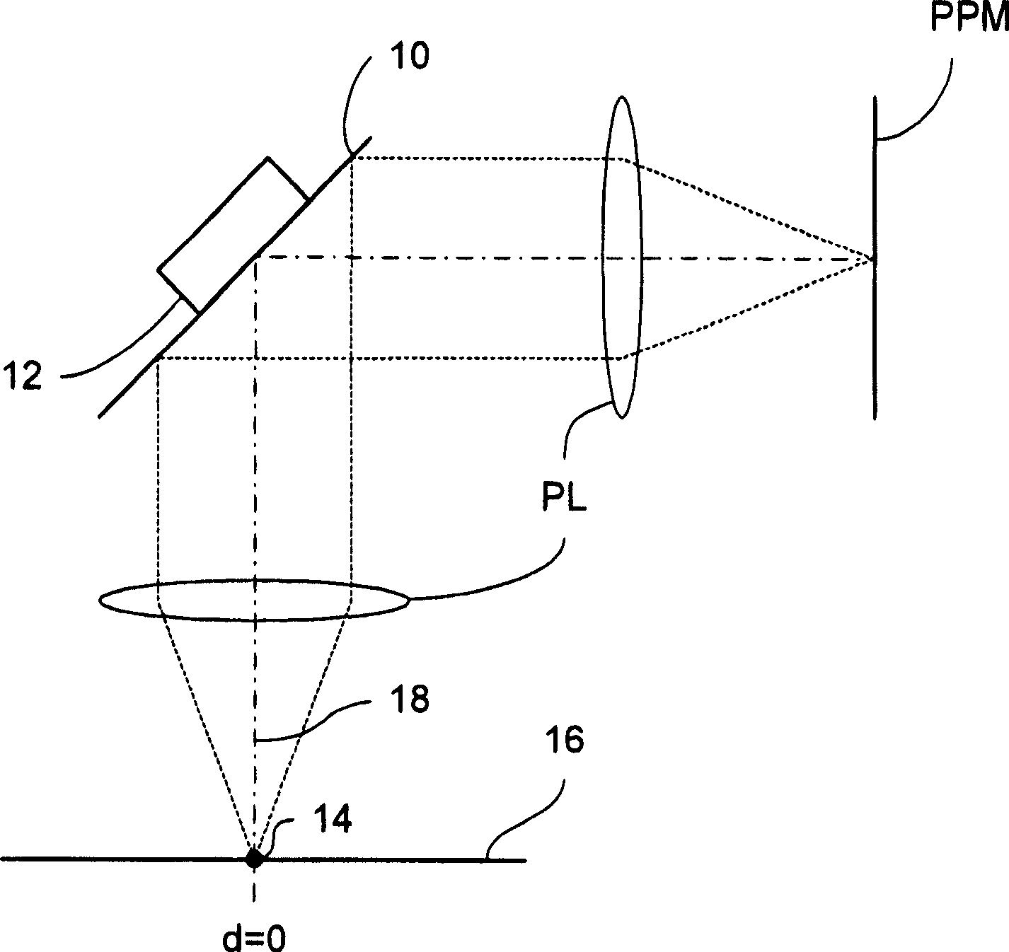
[0046] Embodiments of the invention include, for example, methods and apparatus that can be used to reduce errors caused by movement of a substrate during pulses of a radiation system.
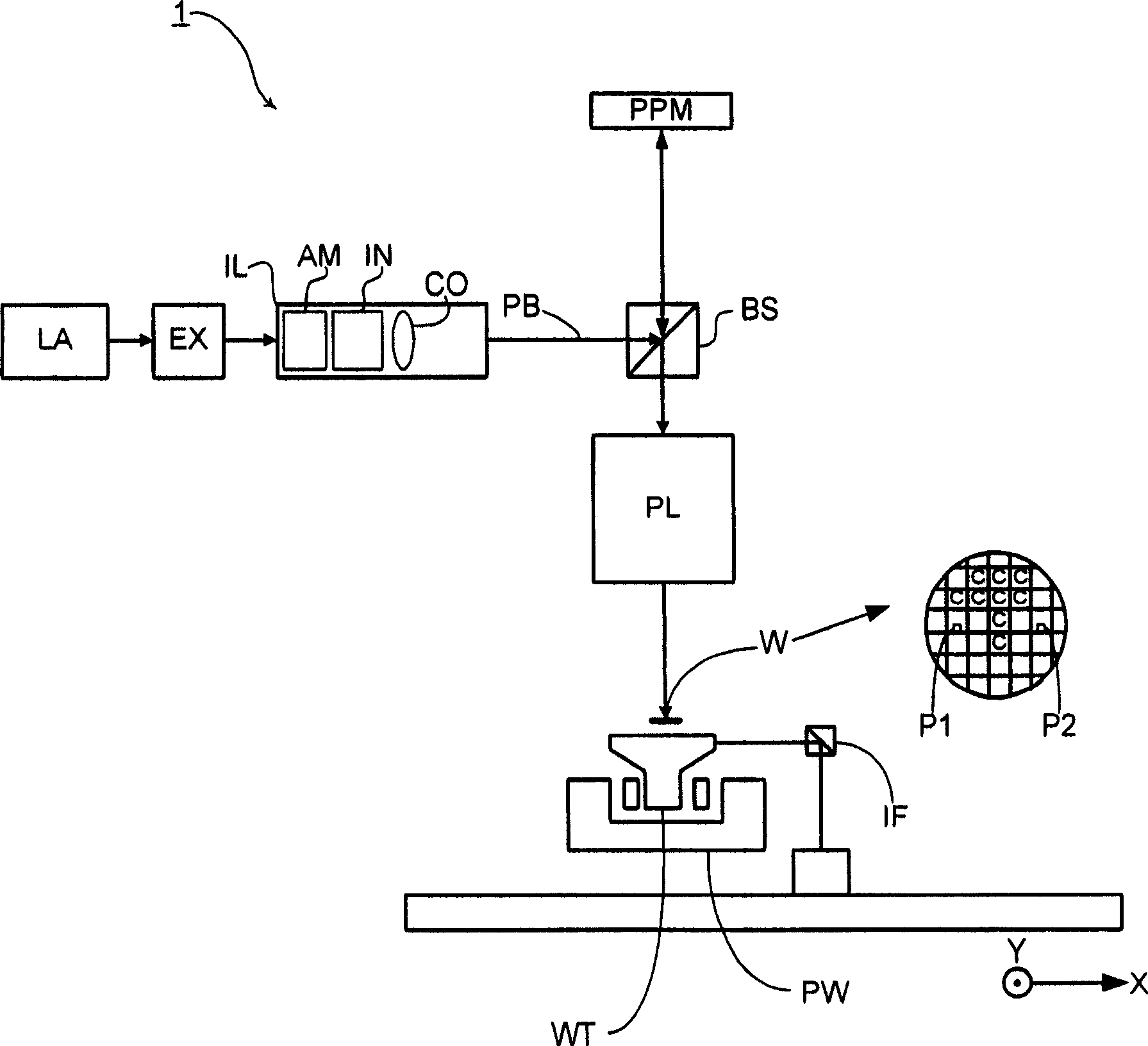
[0047] figure 1 A lithographic projection apparatus 1 according to a particular embodiment of the invention is schematically described, comprising:
[0048] A radiation system for providing a radiation beam (eg, having a structure capable of providing a radiation beam). In this particular example, the radiation system Ex, IL for providing the radiation beam PB (e.g. UV or EUV irradiation) also includes a radiation source LA;
[0049] A programmable patterning structure PPM, such as a programmable mirror array, is configured to apply a pattern to the radiation beam. Typically, the position of the programmable patterning structure is fixed relative to the projection system PL. However, it may alternatively be connected to a positioning structure for its precise positioning relative to the pro...
PUM
 Abstract
Description
Claims
Application Information