Housing for electronic components

A shell and semiconductor technology, applied in the direction of electrical components, electric solid devices, circuits, etc., can solve the problems of poor storage conditions of semiconductor chips, semiconductor chip position deviation, position deviation, etc., to prevent position deviation and realize compactness Size, the effect of reducing the total space

Inactive Publication Date: 2007-07-11
YAMAHA CORP
View PDF1 Cites 4 Cited by
  • Summary
  • Abstract
  • Description
  • Claims
  • Application Information

AI Technical Summary

Problems solved by technology

If the case shakes during transportation, the semiconductor chip may shift in position, resulting in a positional shift or tilt
This results in poor storage conditions for semiconductor chips

Method used


Image

  • Housing for electronic components
  • Housing for electronic components
  • Housing for electronic components

Examples


Embodiment Construction

[0029] The present invention will be described in detail by way of examples with reference to the accompanying drawings.

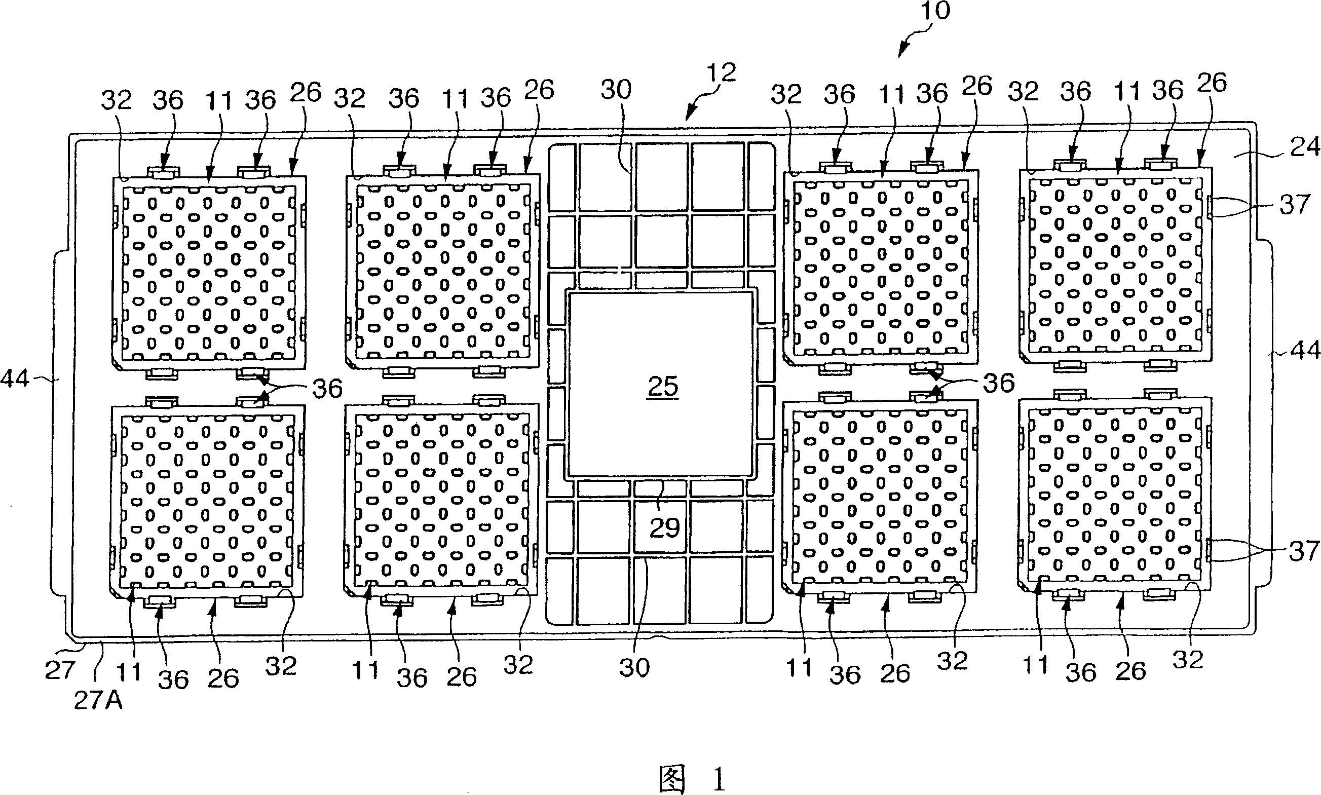
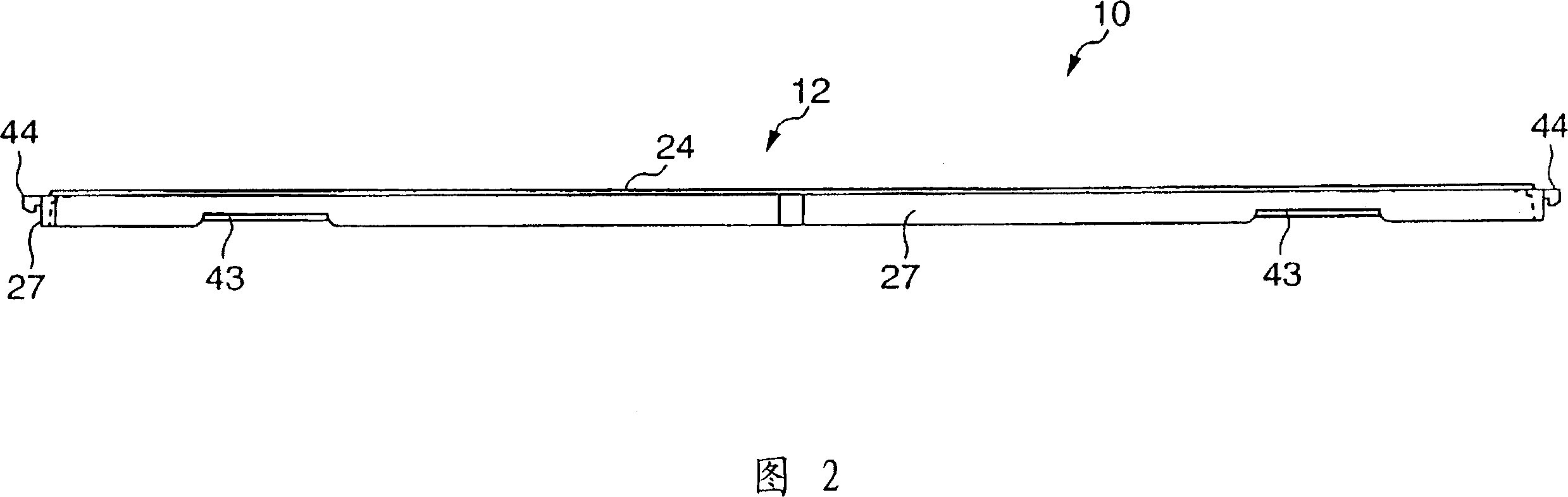
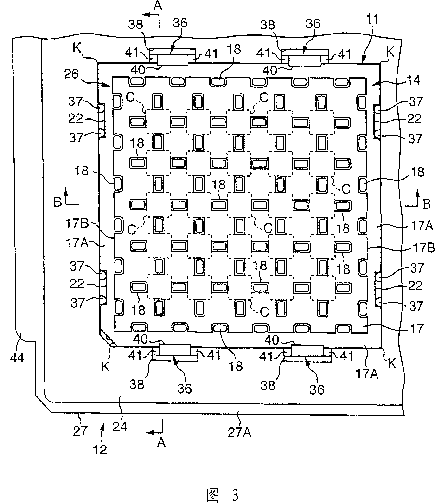
[0030] 1 is a plan view showing a housing including a chip tray and a storage tray according to a preferred embodiment of the present invention; FIG. 2 is a front view of the housing; FIG. 3 is an enlarged view showing basic components of a chip tray; 4C is an enlarged perspective view showing the main part of the casing.

[0031] The housing 10 includes a plurality of chip trays 11 each storing a plurality of chips C and a storage tray 12 storing the chip trays 11 . The present embodiment does not particularly limit the type of chip C; however, the drawings show that the chip C is packaged in a surface mount chip package, such as a BGA (Ball Grid Array) package and a CSP (Chip Scale Package), wherein each chip C Has a two-dimensional square size in which a plurality of terminals are arranged, for example, along one side thereof.

[0032] As shown in FIG...


PUM


Abstract

A housing is disclosed in the invention. A housing is formed in such a way that a plurality of chip trays each holding a plurality of semiconductor chips are stored in a storage tray, wherein the chip tray is formed by vertically connecting an upper unit and a lower unit, both of which have the same structure. The semiconductor chips are held between the upper unit and the lower unit of the chip tray, thus preventing two-dimensional movement thereof. When a plurality of housings each having the aforementioned structure are vertically combined together, a plurality of semiconductor chips can be further held between the upper unit of one housing and the lower unit of another housing. This makes it possible to simultaneously transport numerous semiconductor chips, whereby the semiconductor chips are each encapsulated in a surface mount chip package.

Description

technical field [0001] The present invention relates to housings for storing electronic components such as semiconductor chips therein. Background technique [0002] Conventionally, various types of cases have been used to store and transport components such as semiconductor chips. A typical example of a conventionally known case is designed to include: a plurality of chip trays each holding a plurality of semiconductor chips; and a storage tray larger in size and thickness than the chip tray to store the semiconductor chips. The storage tray has a plurality of containers with open upper ends and stores chip trays. A plurality of protrusions are formed on the upper surface of the chip tray to define areas on which a plurality of semiconductor chips are held such that they are closely held and surrounded by the protrusions and prevented from moving in two-dimensional directions. Chip trays each holding a plurality of semiconductor chips are stored in the container of the st...

Claims


Application Information

Patent Timeline
Patent Type & Authority Applications(China)
IPC IPC(8): H05K5/00H01L23/00
CPCH01L21/67333H01L21/02H01L23/02
Inventor 佐佐木正治
Owner YAMAHA CORP
Why Eureka
Try Eureka