Light emitting device and method of fabricating the same

a technology light emitting diodes, which is applied in the direction of photovoltaic energy generation, semiconductor devices, solid-state devices, etc., can solve the problems of reducing luminous efficacy, reducing reliability and luminous efficacy of light emitting diodes, and generating large amounts of heat for light emitting diodes. , to achieve the effect of preventing the insulation portion from melting, preventing damage, and improving reliability and luminous

Active Publication Date: 2018-06-19
SEOUL VIOSYS CO LTD
View PDF15 Cites 1 Cited by
  • Summary
  • Abstract
  • Description
  • Claims
  • Application Information

AI Technical Summary

Benefits of technology

[0009]Exemplary embodiments of the invention provide a light emitting device capable of effectively dissipating heat while relieving stress applied to a semiconductor layer.

Problems solved by technology

The light emitting diode generates large amounts of heat during light emission.
This causes a decrease in the recombination rate of holes and electrons in the light emitting diode, thereby deteriorating internal quantum efficiency of the light emitting diode and reducing luminous efficacy.
In order to solve this problem, the light emitting diode employs a heat dissipation pad, but still suffers from damage caused by thermal stress applied to the light emitting diode upon light emission.
However, separation of the growth substrate from the semiconductor layers provides a problem of easy damage to a thin semiconductor layer.

Method used


Image

  • Light emitting device and method of fabricating the same
  • Light emitting device and method of fabricating the same
  • Light emitting device and method of fabricating the same

Examples


Embodiment Construction

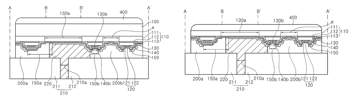
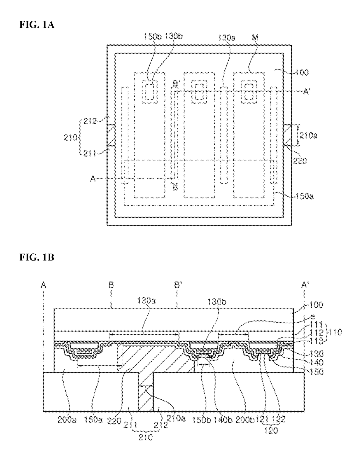
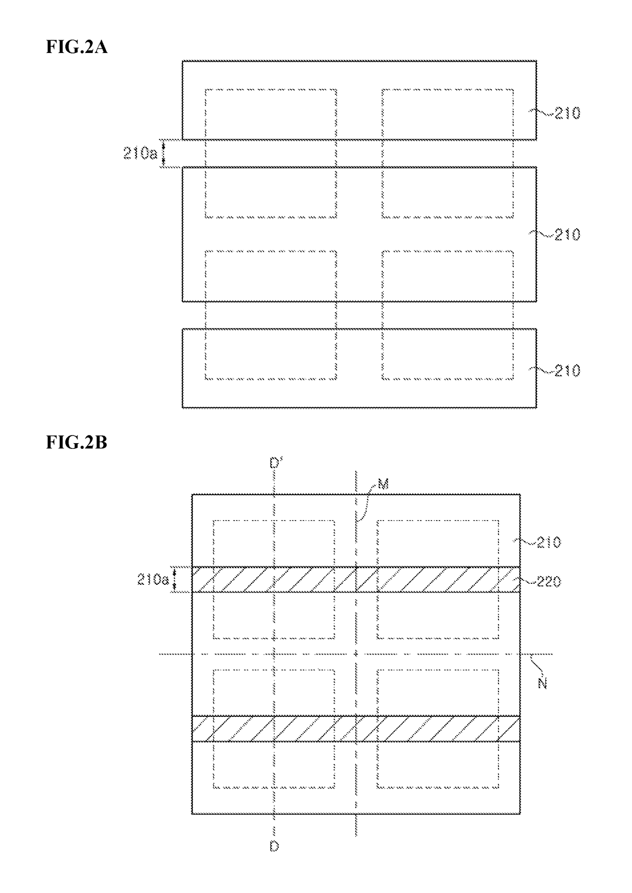
[0071]Hereinafter, exemplary embodiments of the invention will be described in more detail with reference to the accompanying drawings. The following embodiments are provided by way of example so as to fully convey the spirit of the present invention to those skilled in the art to which the present invention pertains. Accordingly, the present invention is not limited to the embodiments disclosed herein and may also be implemented in different forms. In the drawings, widths, lengths, thicknesses, and the like of elements may be exaggerated for clarity and descriptive purposes. When an element or layer is referred to as being “placed on” or “disposed on” another element or layer, it may be directly “placed on” or “disposed on” the other element or layer or intervening elements or layers may be present. Throughout the specification, like reference numerals denote like elements having the same or similar functions.

[0072]FIG. 1A illustrates a light emitting device according to one exempl...


PUM


Abstract

A light emitting device and method of fabricating the same using a wafer level package process are disclosed. The light emitting device has improved heat dissipation to prevent damage by heat, thereby achieving improvement in reliability and luminous efficacy. In addition, the light emitting device has a small difference in coefficients of thermal expansion and thus can reduce stress applied to a light emitting structure to prevent damage to the light emitting structure, thereby achieving improvement in reliability and luminous efficacy.

Description

CROSS-REFERENCE TO RELATED APPLICATIONS[0001]This application is the National Stage Entry of International Patent Application No. PCT / KR2015 / 009172, filed on Sep. 1, 2015, and claims priority from and the benefit of Korean Patent Application No. 10-2014-0129008, filed on Sep. 26, 2014, each of which are incorporated by reference for all purposes as if fully set forth herein.BACKGROUND[0002]Field[0003]The present invention relates to a light emitting device and a method of fabricating the same, and more particularly, to a method of fabricating a light emitting device in which a metal bulk is formed on an electrode, and a light emitting device fabricated by the same.[0004]Discussion of the Background[0005]A light emitting diode (LED) is a solid state device capable of converting electric energy into light, and generally includes an active layer of at least one semiconductor material interposed between semiconductor layers doped with opposite conductive type impurities. When bias is ap...

Claims


Application Information

Patent Timeline
Patent Type & Authority Patents(United States)
IPC IPC(8): H01L51/50H01L51/44H01L33/46H01L33/00H01L33/44
CPCH01L51/504H01L33/46H01L51/442H01L33/0079H01L33/44H01L33/20H01L33/22H01L33/38H01L33/62Y02E10/549H01L33/0093H10K50/13H10K30/82
Inventor JANG, JONG MINCHAE, JONG HYEONSUH, DAE WOONG
Owner SEOUL VIOSYS CO LTD
Why Eureka
Try Eureka