Diode, junction field effect transistor, and semiconductor device
a junction field effect transistor and transistor technology, applied in the field of integrated circuits, to achieve the effect of increasing the reliability of the produ
- Summary
- Abstract
- Description
- Claims
- Application Information
AI Technical Summary
Benefits of technology
Problems solved by technology
Method used
Image
Examples
first embodiment
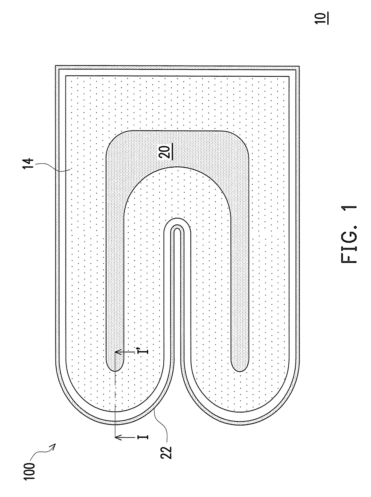
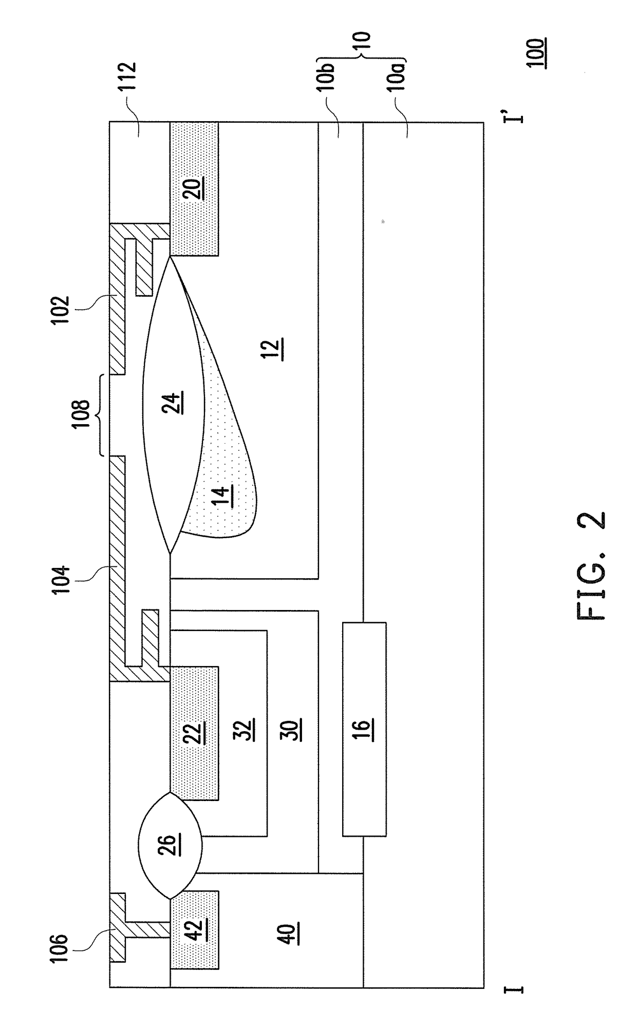
[0025]FIG. 1 is a top view illustrating a diode according to the present disclosure. FIG. 2 is a cross-sectional view taken along a cross-sectional line I-I′ of FIG. 1. For the ease of illustration, only a source, a drain, and a top doped region are illustrated in FIG. 1.
[0026]Referring to FIGS. 1 and 2, generally speaking, a diode device differs from a triode device in that the diode device does not include a gate structure. In the first embodiment of the present disclosure, the diode 100 includes a cathode 20, an anode 22, and a top doped region 14. The cathode 20, the anode 22, and the top doped region 14 are all located in the substrate 10. In another embodiment, the diode 100 may further include a first doped region 12, a second doped region 30, and a third doped region 32.
[0027]The substrate 10 may be a semiconductor substrate 10, such as a silicon substrate. The substrate 10 may be doped with a P-type dopant or an N-type dopant. The P-type dopant may be ions of Group IIIA ele...
second embodiment
[0039]FIG. 3 is a top view illustrating a semiconductor device according to the present disclosure. FIG. 4A is a cross-sectional view taken along a cross-sectional line A-A′ of FIG. 3. FIG. 4B is a cross-sectional view taken along a cross-sectional line B-B′ of FIG. 3. For the ease of illustration, FIG. 3 only illustrates a junction field effect transistor, a high voltage device, a first doped region, a fourth doped region, a first top doped region, a second top doped region, the drain, and the source.
[0040]Referring to FIGS. 3, 4A, and 4B, in the second embodiment, a semiconductor device 110 includes a high voltage device 300 and a junction field effect transistor (JFET) 200 embedded into the high voltage device 300.
[0041]Referring to FIGS. 3 and 4A, in an embodiment, the high voltage device 300 includes the substrate 10, a drain 320, a source 322, a gate structure 316, and a first top doped region 314. In another embodiment, the high voltage device 300 may further include a first ...
third embodiment
[0057]FIG. 5 is a top view illustrating a semiconductor device according to the present disclosure. FIG. 6A is a cross-sectional view taken along a cross-sectional line C-C′ of FIG. 5. FIG. 6B is a cross-sectional view taken along a cross-sectional line D-D′ of FIG. 5. For the ease of illustration, only the substrate, the high voltage device region, the low voltage device region, a termination region, an isolation region, and a drain are illustrated in FIG. 5.
[0058]Referring to FIG. 5, a semiconductor device 120 includes the substrate 10. The substrate 10 has a high voltage device region 400, a low voltage device region 500, a termination region 600, and an isolation region 700. The termination region 600 is located between the high voltage device region 400 and the low voltage device region 500. More specifically, the termination region 600 surrounds the high voltage device 400. In an embodiment, the substrate 10 may also include the semiconductor substrate 10a and the epitaxial la...
PUM
 Abstract
Description
Claims
Application Information


