

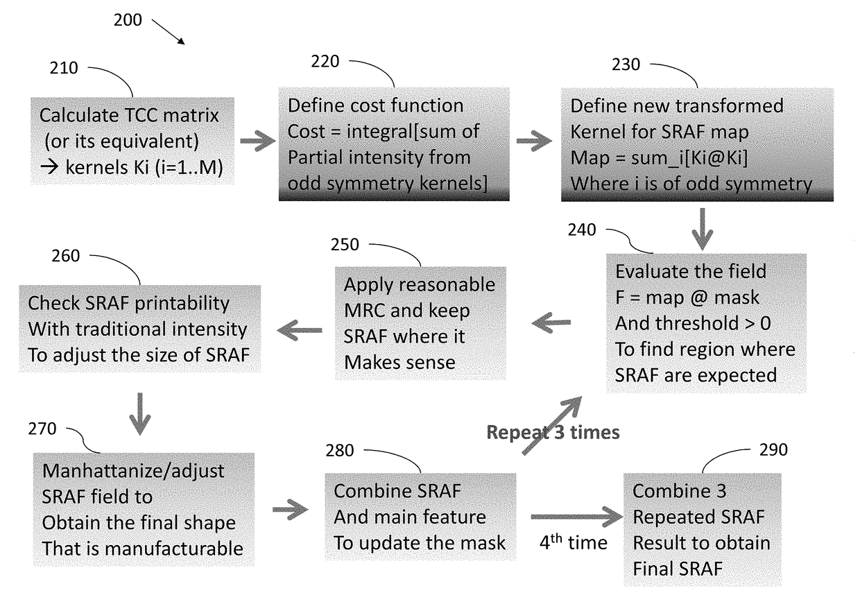
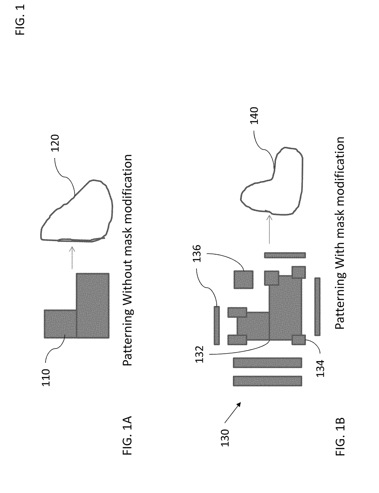
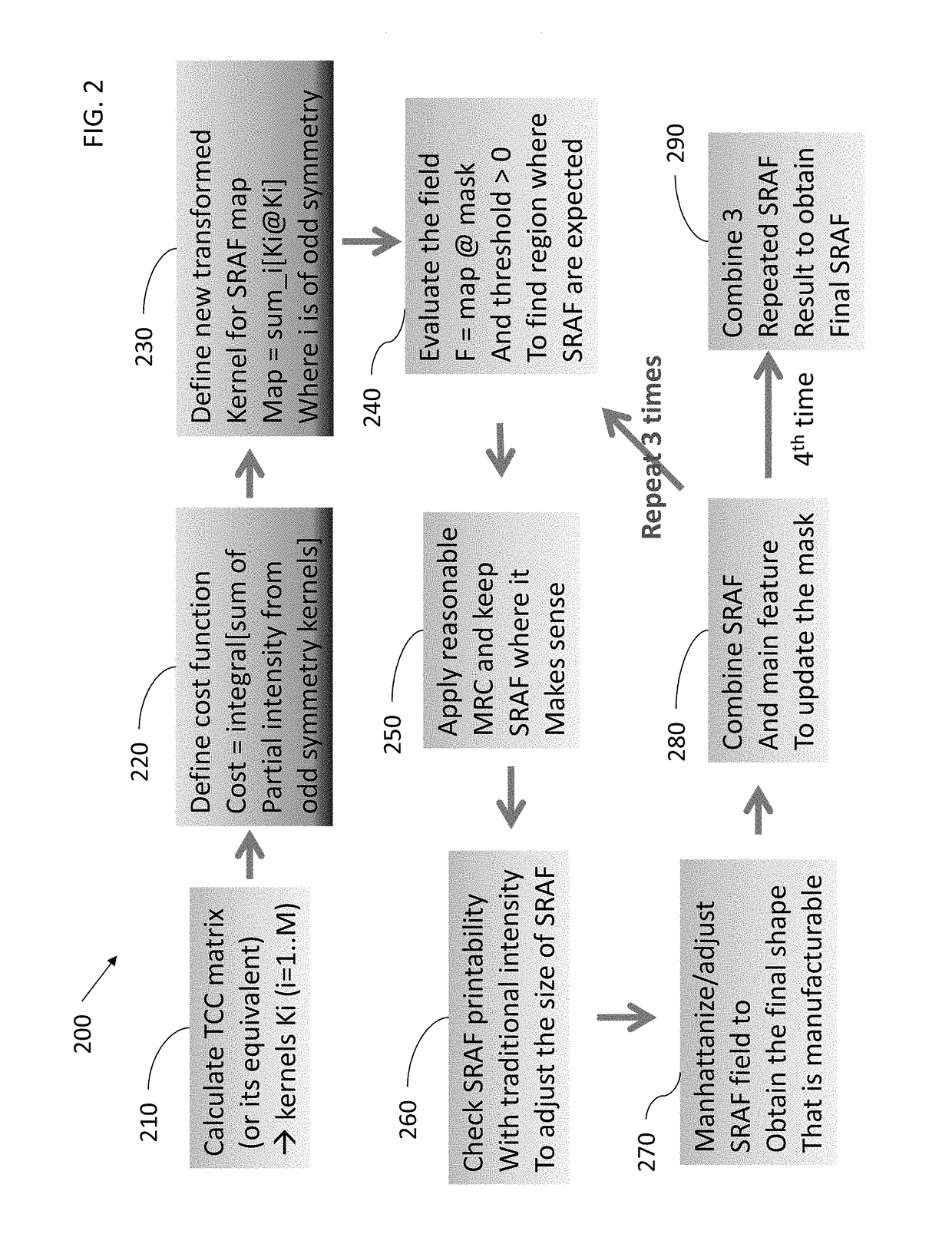
Efficient way to creating process window enhanced photomask layout
a technology of enhanced photomasks and efficient ways, which is applied in the direction of photomechanical equipment, originals for photomechanical treatment, instruments, etc., can solve the problems that features may no longer resemble the pattern of photomasks, and achieve accurate and computationally efficient, simplify the underlying physics, and sufficient accurate results
- Summary
- Abstract
- Description
- Claims
- Application Information
AI Technical Summary
Benefits of technology
Problems solved by technology
Method used
Image

Examples
Embodiment Construction
[0039]Hereinafter, example embodiments will be described in more detail with reference to the accompanying drawings, in which like reference numbers refer to like elements throughout. The present invention, however, may be embodied in various different forms, and should not be construed as being limited to only the illustrated embodiments herein.
[0040]Herein, the use of the term “may,” when describing embodiments of the present invention, refers to “one or more embodiments of the present invention.” In addition, the use of alternative language, such as “or,” when describing embodiments of the present invention, refers to “one or more embodiments of the present invention” for each corresponding item listed.
[0041]The electronic or electric devices and / or any other relevant devices or components according to embodiments of the present invention described herein may be implemented utilizing any suitable hardware, firmware (e.g., an application-specific integrated circuit (ASIC)), softwa...
PUM
| Property | Measurement | Unit |
|---|---|---|
| feature sizes | aaaaa | aaaaa |
| feature sizes | aaaaa | aaaaa |
| light wavelength | aaaaa | aaaaa |
Abstract
Description
Claims
Application Information