Metal wiring bonding structure and production method therefor

a metal wiring and production method technology, applied in the direction of soldering apparatus, furnace heating elements, semiconductor/solid-state device details, etc., can solve the problems of difficult to accurately align the contact pattern and connection failure, and achieve the effect of easy checking of the connection state and easy positioning

Active Publication Date: 2018-07-24
NGK INSULATORS LTD
View PDF1 Cites 2 Cited by
  • Summary
  • Abstract
  • Description
  • Claims
  • Application Information

AI Technical Summary

Benefits of technology

[0014]In this metal wiring bonding structure, since portions of the bonding member that cover the surfaces of the first contact opposed lands and the distal end surface of the first member can be inspected from the outside, the connection state can be checked easily, and bonding members in a good contact state can be selected. Further, in a case in which the first contacts of the first member are positioned to be opposed to the second contacts of the second member, when the first member is placed on the second member, the extended surfaces of the second contacts and the first contact opposed lands are both seen from above the first member. Hence, positioning can be easily performed by utilizing the first contact opposed lands and the extended surfaces of the second contacts. In this way, bonding members in a good connection state can be selected by inspection from the outside, and the first contacts and the second contacts can be aligned easily. Therefore, it is possible to provide the metal wiring bonding structure in which the first member having the first contacts and the second member having the second contacts are properly bonded. Here, the term “brazing and soldering” refers to soldering (the melting temperature is less than 450° C.) and brazing (the melting temperature is 450° C. or more).
[0015]In the metal wiring bonding structure of the present invention, the first contact opposed lands may extend to the distal end surface of the first member. This allows the melted solder to be easily supplied from the first contact opposed lands to the bonding space via the distal end surface of the first member and the extended surface of the second contacts.
[0023]In this production method for the metal wiring bonding structure, the first member is placed on the second member, and the first member and the second member are aligned by utilizing the first contact opposed lands and the extended surfaces of the second contacts so that the first contacts are opposed to the base surfaces of the second contacts. The first contacts are provided on a back side of the first contact opposed lands, and the base surfaces are provided to continue from the extended surfaces of the second contacts. Moreover, the first contact opposed lands and the extended surfaces of the second contacts can both be checked from above the first member. For this reason, alignment can be easily performed by utilizing the first contact opposed lands and the extended surfaces of the second contacts so that the first contacts are opposed to the base surfaces of the second contacts. Further, the bonding member formed by hardening the melted brazing and soldering material covers the surfaces of the first contact opposed lands, the distal end surface of the first member, and the extended surfaces of the second contacts, and is filled in the bonding space between the first contacts and the second contacts. Since portions of the bonding member that cover the surfaces of the first contact opposed lands and the distal end surface of the first member can be inspected from the outside, the connection state can be easily checked, and bonding members in a good connection state can be selected. In this way, bonding members in the good connection state can be selected by inspection from the outside, and the first contacts and the second contacts can be aligned easily. Therefore, it is possible to provide the metal wiring bonding structure in which the first member having the first contacts and the second member having the second contacts are properly bonded.

Problems solved by technology

However, in the bonding structure of FIG. 9, since the position of the contact pattern 114 cannot be checked from above the flexible board 110, it is difficult to accurately align the contact pattern 114 and the contact pattern 124.
Also, when the solder is melted, heat does not spread over the entire solder, and this sometimes causes connection failure.

Method used


Image

  • Metal wiring bonding structure and production method therefor
  • Metal wiring bonding structure and production method therefor
  • Metal wiring bonding structure and production method therefor

Examples


Embodiment Construction

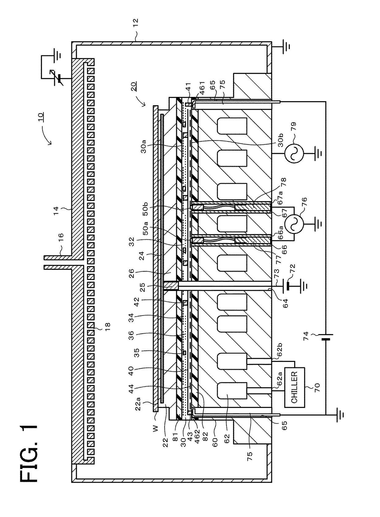
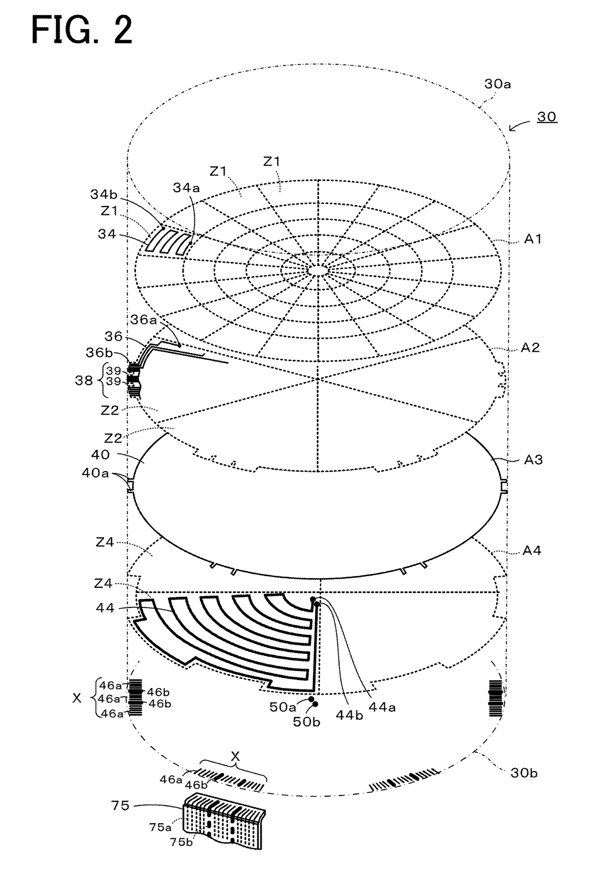
[0033]A preferred embodiment of the present invention will be described below with reference to the drawings. FIG. 1 is a cross-sectional view illustrating a schematic configuration of a plasma treatment apparatus 10, and FIG. 2 is a perspective view illustrating an internal structure of a sheet heater 30.

[0034]As illustrated in FIG. 1, the plasma treatment apparatus 10 serving as a semiconductor manufacturing apparatus includes a vacuum chamber 12, a shower head 14, and an electrostatic chuck heater 20. The vacuum chamber 12 is a box-shaped container formed of, for example, an aluminum alloy. The shower head 14 is provided in a ceiling surface of the vacuum chamber 12. The shower head 14 releases process gas supplied from a gas introduction pipe 16 into the vacuum chamber 12 through multiple gas injection ports 18. Also, the shower head 14 functions as a cathode plate for plasma generation. The electrostatic chuck heater 20 is a device that attracts and holds a wafer W on a wafer m...


PUM

PropertyMeasurementUnit
melting temperatureaaaaaaaaaa
thicknessaaaaaaaaaa
bonding structureaaaaaaaaaa

Abstract

A metal wiring bonding structure 100 comprises contacts 753 of connection FPC 75 and heater lands 46 of a sheet heater 30 to be bonded by a solder bonding member 766. A connection FPC 75 includes contact opposed lands 754 formed of metal and disposed at positions respectively opposed to the plurality of contacts 753 on a surface of a support layer 751 opposite from a surface on which metal wires 750 are provided. In addition to base surfaces 461 opposed to the contacts 753, the heater lands 46 respectively include extended surfaces 462 opposed to imaginary extended portions 753b imaginarily extended ahead from the contacts 753. A solder bonding member 756 covers surfaces of the contact opposed lands 754, a distal end surface of the connection FPC 75, and the extended surfaces 462 of the heater lands 46, and is filled in a bonding space C.

Description

[0001]The present application claims priority from U.S. Provisional Application No. 62 / 314,547 and U.S. Provisional Application No. 62 / 314,556, filed on Mar. 29, 2016, and Japanese Patent Application No. 2016-128765 and Japanese Patent Application No. 2016-128766, filed on Jun. 29, 2016, the entire contents of which are incorporated herein by reference.BACKGROUND OF THE INVENTION1. Field of the Invention[0002]The present invention relates to a metal wiring bonding structure and a production method therefor.2. Description of the Related Art[0003]In a conventionally known structure for bonding a flexible board and a printed board, a contact part, such as a contact pattern, on the flexible board and a corresponding contact part on the printed board are electrically connected by soldering (for example, PTL 1). FIG. 9 illustrates an example of such a bonding structure. A coverlay film 112 is removed from a board end of a flexible board 110, where end portions of copper foil patterns arra...

Claims


Application Information

Patent Timeline
Patent Type & Authority Patents(United States)
IPC IPC(8): B23K1/00H05B3/62H01L21/00H01L23/00B23K20/00H01L21/683H05K1/02H05K1/11H01L21/67B23K101/42
CPCB23K20/004B23K1/0016H01L21/67103H01L21/6831H05B3/62H05K1/028H05K1/118H01L21/6833H01L21/67069B23K2201/42H01R12/62H05B3/143H05K3/34B23K3/04B23K2101/42H01R43/02H05K1/0212H05K3/3494H05K3/363
Inventor KIN, RISHUNTAKEBAYASHI, HIROSHIHIRATA, NATSUKI
Owner NGK INSULATORS LTD
Why Eureka
Try Eureka