Supercharge Your Innovation With Domain-Expert AI Agents!

Threshold voltage adjustment of a transistor

a technology of mos transistor and threshold voltage, which is applied in the direction of transistors, semiconductor devices, electrical equipment, etc., can solve the problems of increasing the cost of circuit fabrication, increasing the leakage current,

Active Publication Date: 2018-07-24
MICRON TECH INC
View PDF44 Cites 0 Cited by
  • Summary
  • Abstract
  • Description
  • Claims
  • Application Information

AI Technical Summary

Benefits of technology

The present invention provides methods for adjusting the threshold voltage of long-channel transistors that are optimized for short-channel transistors. These methods involve forming a layer of gate oxide over at least a part of the channel region with a gate formed over the gate oxide. The gate includes at least one aperture formed therein with the channel region of the substrate further including an implanted region within the channel between the source and drain regions. The invention also includes methods for manufacturing an MOS structure on a semiconductor substrate by patterning a first mask layer followed by etching to form a gate with an aperture between the source and drain ends of the polysilicon layer. Implant regions are formed in the substrate adjacent to the drain and source ends of the gate and at least one implant region is formed in the substrate through the aperture of the gate. The technical effect of the invention is to provide improved performance and stability of long-channel transistors that are optimized for short-channel transistors.

Problems solved by technology

Furthermore, the reduced threshold voltages of the longer channel devices lead to increased leakage currents which, in turn, are particularly undesirable in circuits that are utilized in battery-operated devices.
One shortcoming to the multiple-threshold adjusting implant approach, however, is that utilizing separate implant steps requires separate masks which, in turn, increases the cost of fabricating the circuit.

Method used


Image

  • Threshold voltage adjustment of a transistor
  • Threshold voltage adjustment of a transistor
  • Threshold voltage adjustment of a transistor

Examples


Embodiment Construction

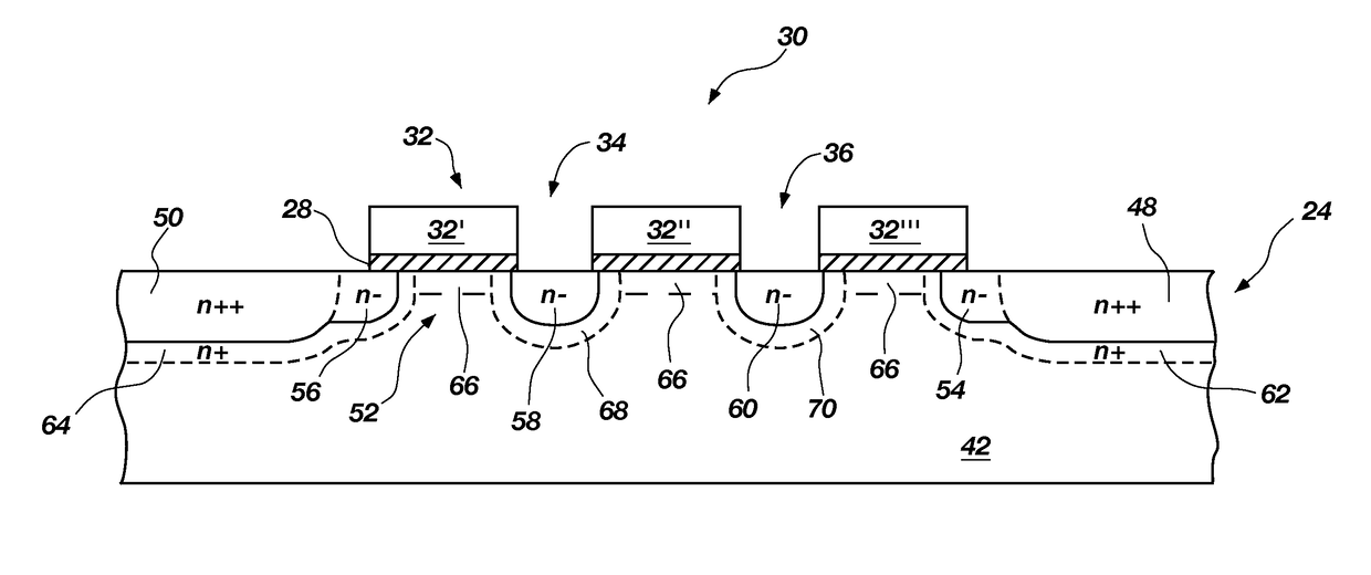
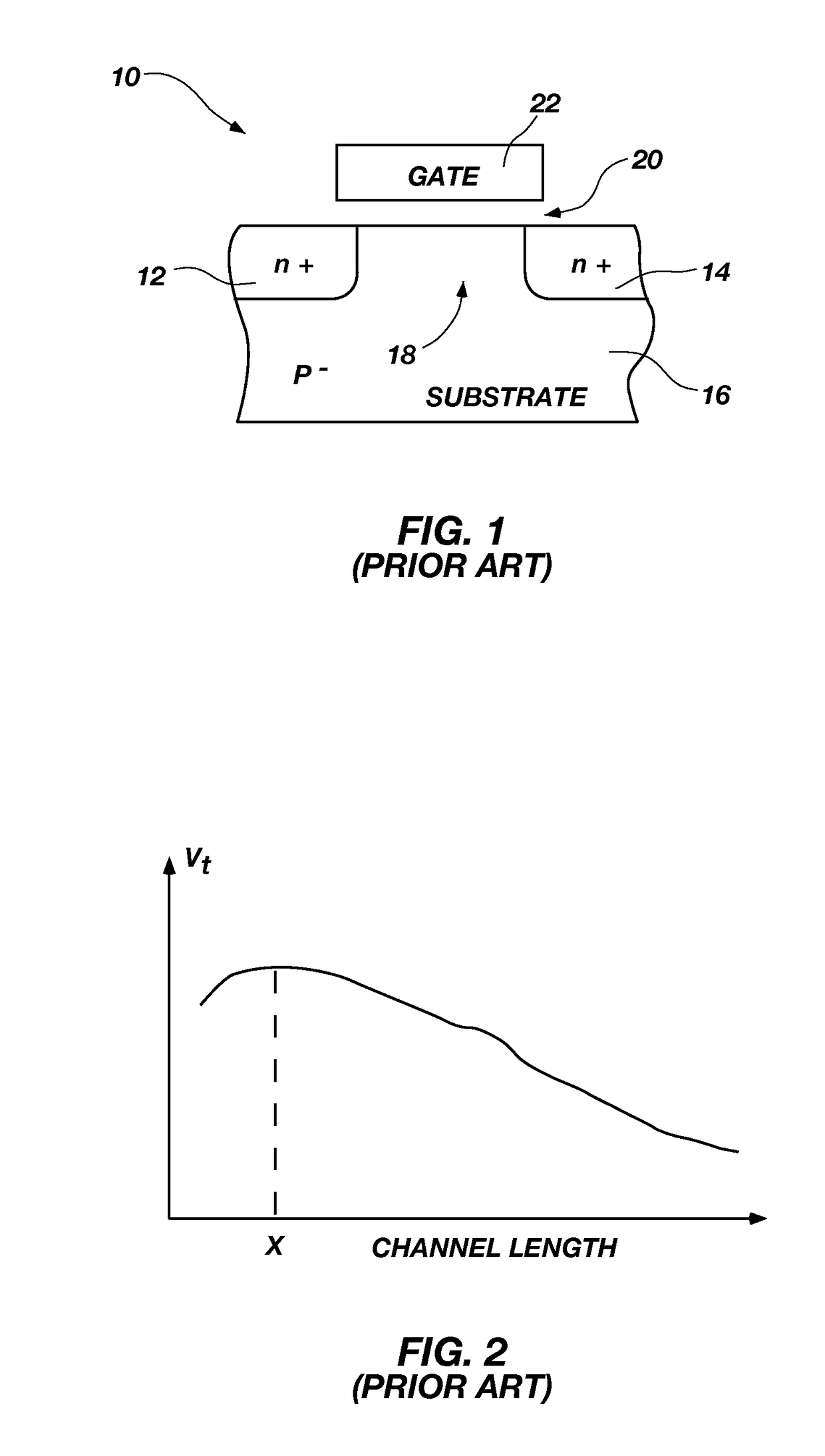
[0026]While short-channel transistors are susceptible to decreased threshold voltages and therefore utilize threshold voltage adjusting enhancement implants for adjusting the threshold voltage, short-channel transistors are also susceptible to so-called “hot carrier effects.” Generally, as the channel length is shortened, the maximum electric field Em becomes more isolated near the drain side of the channel, causing a saturated condition that increases the maximum energy on the drain side of the MOS device. The high energy causes electrons in the channel region to become “hot.” An electron generally becomes hot in the vicinity of the drain edge of the channel where the energy arises. Hot electrons can degrade device performance and cause breakdown of the device. Moreover, the hot electrons can overcome the potential energy barrier between the silicon substrate and the silicon dioxide layer overlying the substrate, which causes hot electrons to be injected into the gate oxide.

[0027]P...


PUM


Abstract

A threshold voltage adjusted long-channel transistor fabricated according to short-channel transistor processes is described. The threshold-adjusted transistor includes a substrate with spaced-apart source and drain regions formed in the substrate and a channel region defined between the source and drain regions. A layer of gate oxide is formed over at least a part of the channel region with a gate formed over the gate oxide. The gate further includes at least one implant aperture formed therein with the channel region of the substrate further including an implanted region within the channel between the source and drain regions. Methods for forming the threshold voltage adjusted transistor are also disclosed.

Description

CROSS-REFERENCE TO RELATED APPLICATIONS[0001]This application is a continuation of U.S. patent application Ser. No. 13 / 155,029, filed Jun. 7, 2011, now U.S. Pat. No. 9,111,958, issued Aug. 18, 2015, which application is a divisional of U.S. patent application Ser. No. 11 / 932,209, filed Oct. 31, 2007, now U.S. Pat. No. 7,968,411, issued Jun. 28, 2011, which is a continuation of U.S. patent application Ser. No. 11 / 081,336, filed Mar. 16, 2005, now U.S. Pat. No. 7,422,948, issued Sep. 9, 2008, which is a divisional of U.S. patent application Ser. No. 10 / 690,399, filed Oct. 20, 2003, now U.S. Pat. No. 7,274,076, issued Sep. 25, 2007, the disclosure of each of which is hereby incorporated herein in its entirety by this reference.BACKGROUND[0002]Field of the Invention[0003]The present invention relates to semiconductor devices and, more particularly, to threshold voltage adjustment of long-channel MOS transistors.[0004]State of the Art[0005]Metal-Oxide-Semiconductor (MOS) is the primary t...

Claims


Application Information

Patent Timeline
Patent Type & Authority Patents(United States)
IPC IPC(8): H01L29/78H01L21/8238H01L29/66H01L21/265H01L21/8234H01L21/336
CPCH01L29/7816H01L21/26586H01L21/823412H01L21/823807H01L29/7831H01L29/6659H01L29/66484H01L29/66537H01L29/66681H01L29/6653
Inventor WILLIFORD, ETHAN
Owner MICRON TECH INC
Features
  • R&D
  • Intellectual Property
  • Life Sciences
  • Materials
  • Tech Scout
  • Unparalleled Data Quality
  • Higher Quality Content
  • 60% Fewer Hallucinations
Learn More