
AMOLED display device

a display device and amoled technology, applied in the field of amoled display devices, can solve the problems of poor display performance and large power loss, and achieve the effect of lowering the ir drop of the display circui

Active Publication Date: 2018-09-11
TCL CHINA STAR OPTOELECTRONICS TECH CO LTD
View PDF2 Cites 1 Cited by
  • Summary
  • Abstract
  • Description
  • Claims
  • Application Information

AI Technical Summary

Benefits of technology

[0007]An objective of the present invention is to provide an active matrix organic light-emitting diode (AMOLED) display device, which helps lower down IR drop in a display circuit, without affecting overall pixel arrangement of the AMOLED display device.
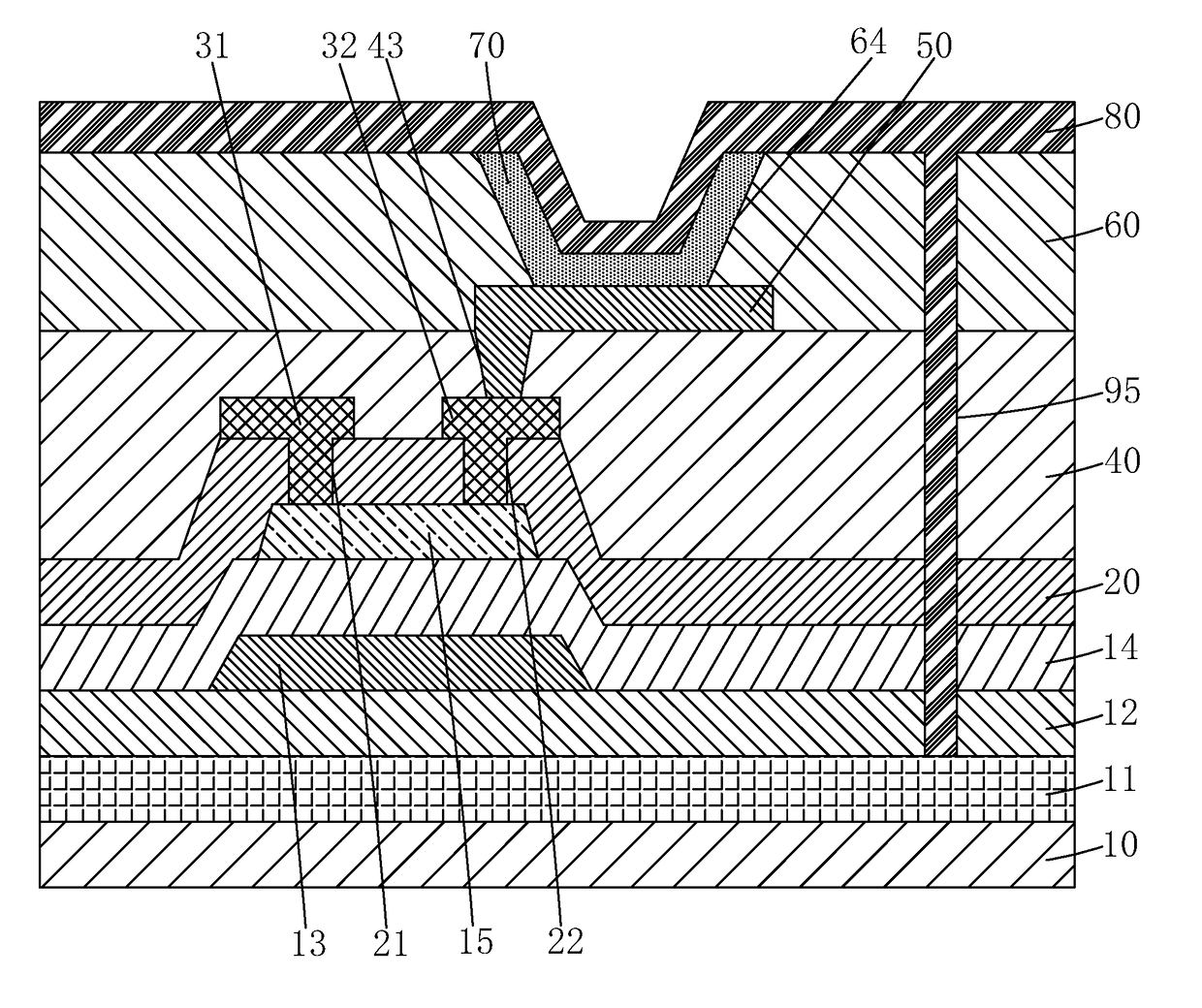
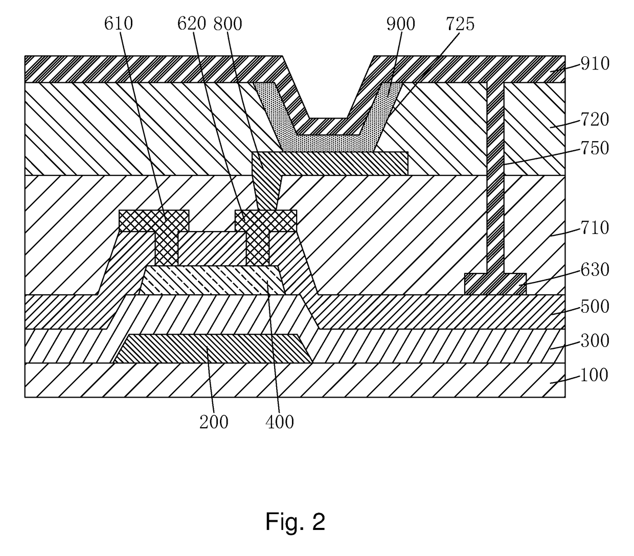
[0025]The efficacy of the present invention is that the present invention provides an AMOLED display device, which comprises a cathode connection layer formed on a backing plate and provides connection between the cathode and the cathode connection layer through a via formed in and through structural layers thereof so that in a normal displaying operation of the AMOLED display device, an electrical current signal is conducted through the cathode connection layer to a cathode, achieving transmission of the electrical current signal through an interior of each pixel to the cathode, and making a conduction path of the electrical current signal shortened as compared to a conventional AMOLED display device and reducing electrical resistance of the conduction path of the electrical current signal, thereby lowering IR drop of a display circuit and helping improve displaying performance and power loss of the AMOLED display device. Further, since the cathode connection layer is disposed on the backing plate and the connection between the cathode and the cathode connection layer requires only one via, no much space of pixel arrangement will be occupied and thus no significant influence will be imposed on the entire pixel arrangement of the AMOLED display device.

Problems solved by technology

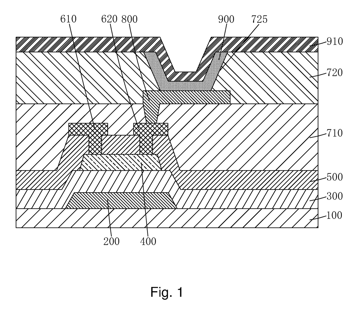
In other words, an electrical voltage that is actually transmitted to the cathode 910 is lower than a voltage set for it so that the display performance would be poor and power loss would be large.

Method used


Image

  • AMOLED display device
  • AMOLED display device
  • AMOLED display device

Examples


Embodiment Construction

[0033]To further expound the technical solution adopted in the present invention and the advantages thereof, a detailed description will be given with reference to the preferred embodiments of the present invention and the drawings thereof.

[0034]Referring to FIG. 3, the present invention provides an active matrix organic light-emitting diode (AMOLED) display device, which comprises: a backing plate 10, a cathode connection layer 11 disposed on the backing plate 10, a buffer layer 12 disposed on the cathode connection layer 11, a gate electrode 13 disposed on the buffer layer 12, a gate insulation layer 14 disposed on the gate electrode 13 and the buffer layer 12, an active layer 15 disposed on the gate insulation layer 14 and located above and corresponding to the gate electrode 13, an etch stop layer 20 disposed on the active layer 15 and the gate insulation layer 14, a first via 21 and a second via 22 formed in the etch stop layer 20 and respectively corresponding to two opposite ...


PUM


Abstract

The present invention provides an AMOLED display device, which includes a cathode connection layer formed on a backing plate and provides connection between the cathode and the cathode connection layer through a via formed in and through structural layers thereof so that in a normal displaying operation of the AMOLED display device, an electrical current signal is conducted through the cathode connection layer to a cathode, achieving transmission of the electrical current signal through an interior of each pixel to the cathode, and making a conduction path of the electrical current signal shortened as compared to a conventional AMOLED display device and reducing electrical resistance of the conduction path of the electrical current signal, thereby lowering IR drop of a display circuit and helping improve displaying performance and power loss of the AMOLED display device. Further, since the cathode connection layer is disposed on the backing plate and the connection between the cathode and the cathode connection layer requires only one via, no much space of pixel arrangement will be occupied and thus no significant influence will be imposed on the entire pixel arrangement of the AMOLED display device.

Description

BACKGROUND OF THE INVENTION1. Field of the Invention[0001]The present invention relates to the field of display technology, and more particular to an active matrix organic light-emitting diode (AMOLED) display device.2. The Related Arts[0002]Organic light-emitting diode (OLED) displays, which are also referred to organic electroluminescent displays, are a newly emerging flat panel display device and possess advantages, such as being self-luminous, low drive voltage, high luminous brightness, short response time, high clarity and contrast, almost 180° view angle, wide range of operation temperature, and easy realization of flexible displaying and large-area full-color displaying, and are considered the most promising display devices.[0003]Based on the way of driving, OLEDs can be classified in two categories, passive matrix OLED (PMOLED) and active matrix OLED (AMOLED), namely one for direct addressing, and the other for TFT array addressing, among which, the AMOLED comprises pixels ...

Claims


Application Information

Patent Timeline
Patent Type & Authority Patents(United States)
IPC IPC(8): H01L27/32H01L51/52H01L51/50
CPCH01L27/3276H01L51/5012H01L51/5056H01L51/5221H01L51/5092H01L51/5218H01L51/5072H01L27/124H01L27/127H10K59/123H10K59/1315H01L27/1248H10K59/131H10K50/824H10K50/11H10K50/15H10K50/16H10K50/82H10K50/171H10K50/818
Inventor HAN, BAIXIANG
Owner TCL CHINA STAR OPTOELECTRONICS TECH CO LTD
Learn More