

Semiconductor device and method for manufacturing the same
a technology of semiconductor devices and semiconductors, applied in semiconductor devices, semiconductor/solid-state device details, electrical apparatus, etc., can solve the problems of short-circuiting between chips, and achieve the effect of preventing the bridging over of bonding materials to adjacent islands, high reliability, and preventing short-circuiting between islands
Active Publication Date: 2018-10-02
ROHM CO LTD
View PDF18 Cites 0 Cited by
- Summary
- Abstract
- Description
- Claims
- Application Information
AI Technical Summary
Benefits of technology
The present invention provides a semiconductor device and a method for manufacturing it that prevents short-circuiting between semiconductor chips due to bridging of bonding material. The semiconductor device includes a plurality of islands with plating layers formed on their outer surfaces, where the peripheral edge portion at the first end surface of an island is masked to prevent the formation of plating layers on that surface. This prevents the bonding material from wet-spreading to the first end surface and avoids bridging over to an adjacent island, resulting in a semiconductor device with high reliability.
Problems solved by technology
When a plurality of semiconductor chips are mounted in a single resin package as in Patent Document 1, there is a problem of short-circuiting between the chips.
Method used
View moreImage
Smart ImageViewing Examples

Examples
examples
[0068]Although the present invention shall now be described based on an example and a comparative example, the present invention is not restricted by the example described below.
example
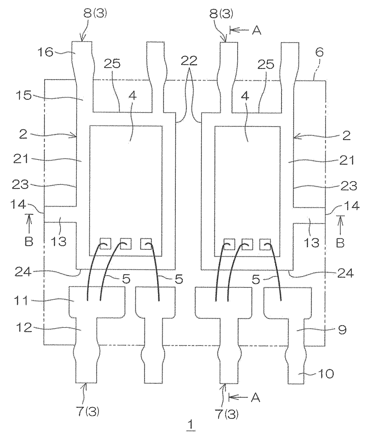
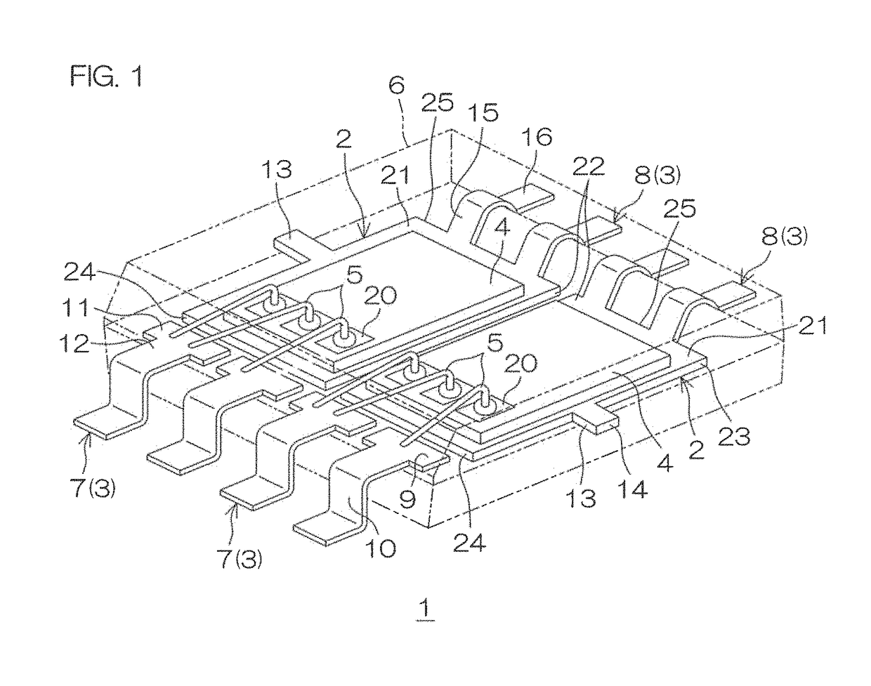
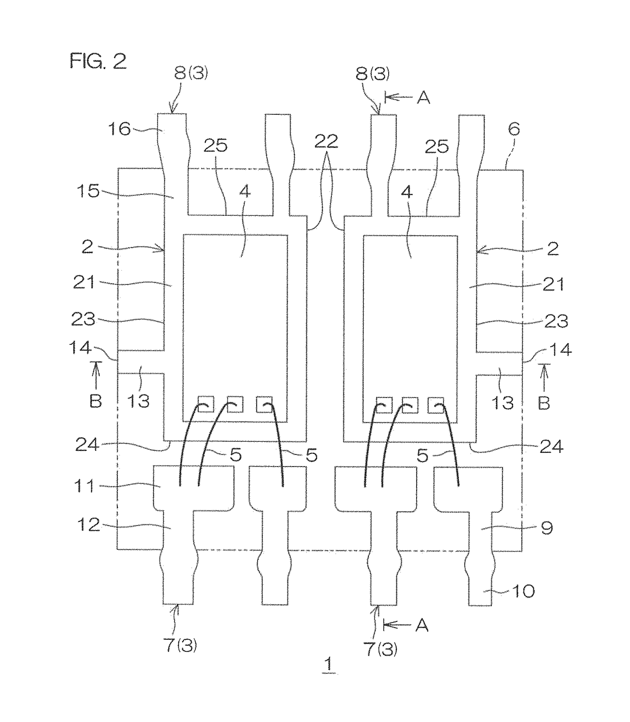
[0069]A semiconductor device 1 was prepared in accordance with the preferred embodiment described above. Here, a bare surface region 27 was formed on the facing end surface 22 of one island 2 of the two islands 2 and a plating film 17 was formed on the other facing end surface 22. The main constituent materials were as follows:[0070]Islands 2 and leads 3: Cu alloy[0071]Plating film 17: Ag plating film[0072]Bonding material 32: Pb-3Sn-1Ag solder
Login to View More PUM
 Abstract
A semiconductor device includes a plurality of islands, each having an outer surface including an upper surface and end surfaces, semiconductor chips, above the respective islands, a bonding material, between the islands and the semiconductor chips, and plating layers, formed on the outer surfaces of the islands, and with at least one of the plurality of islands, the island is exposed as a bare surface region at a first end surface, which, among the end surfaces of the one island, faces the island adjacent thereto.
Description
CROSS-REFERENCE TO RELATED APPLICATIONS[0001]The present application corresponds to Japanese Patent Application No. 2016-81468 filed in the Japan Patent Office on Apr. 14, 2016, and the entire disclosure of this application is incorporated herein by reference.TECHNICAL FIELD[0002]The present invention relates to a semiconductor device and a method for manufacturing the same.BACKGROUND ART[0003]For example, Patent Document 1 (Japanese Patent Application Publication No. 6-61406) discloses a semiconductor device, including a plurality of islands, a plurality of semiconductor chips, mounted above the respective islands using an Ag-based material, etc., and a resin package that collectively seals the plurality of islands and plurality of semiconductor chips.SUMMARY OF INVENTION[0004]When a plurality of semiconductor chips are mounted in a single resin package as in Patent Document 1, there is a problem of short-circuiting between the chips. For example, a bonding material bonding a semic...
Claims
Login to View More Application Information
Patent Timeline
 Patent Type & AuthorityPatents(United States)
IPC IPC(8): H01L23/495H01L23/00H01L23/31H01L21/48H01L21/56
CPCH01L23/49548H01L21/565H01L23/3114H01L23/4952H01L23/49513H01L23/49575H01L23/49582H01L24/27H01L24/32H01L24/48H01L24/73H01L21/4825H01L2224/73265H01L2224/27462H01L2224/27472H01L2224/32245H01L2224/48245H01L23/3107H01L23/49503H01L23/49541H01L24/29H01L24/45H01L24/49H01L24/83H01L24/92H01L2224/05554H01L2224/29101H01L2224/29116H01L2224/45124H01L2224/45144H01L2224/45147H01L2224/48247H01L2224/48465H01L2224/49113H01L2224/83026H01L2224/83439H01L2224/85439H01L2224/92247H01L2924/13091H01L2924/181H01L2924/00014H01L2924/01204H01L2924/00012H01L2924/014H01L2924/013H01L2924/01047H01L2924/0105H01L2924/00
InventorHAGA, MOTOHARUFUTAMURA, YOSUI
OwnerROHM CO LTD