Low power voltage level shifter circuit

a voltage level shifter and low-power technology, applied in logic circuits, logic circuit coupling/interface arrangements, pulse techniques, etc., can solve the problems of significant current draw from power supplies and applications that do not have the available power to provide this switching current, and achieve the effect of limiting the amount of power consumed

Active Publication Date: 2018-10-16
SYNOPSYS INC
View PDF14 Cites 2 Cited by
  • Summary
  • Abstract
  • Description
  • Claims
  • Application Information

AI Technical Summary

Benefits of technology

[0007]The present invention also provides for a voltage level shifter circuit in an integrated circuit. The voltage level shifter circuit has a first voltage level driver circuit receiving signals within a first voltage level, the first voltage level driver circuit operating at a first voltage level and connected to a first voltage power supply; a protection logic circuit receiving signals from the first voltage level driver circuit and shifting the first logic level signals to second logic level signals; a second voltage level logic circuit receiving signals from the protection logic circuit, the second voltage level logic circuit operating at a second voltage level and connected to a second voltage power supply; a bias voltage generator circuit; and at least one current-limiting MOS transistor connected between the second voltage level logic circuit and the second voltage power supply, the at least one current-limiting transistor responsive to a bias voltage from the bias voltage generator circuit to provide a set current through the second voltage level logic circuit to limit the amount of power consumed by the second voltage level logic circuit.

Problems solved by technology

A problem with a conventional voltage level shifter is that during the time when the level shifter is switching, there is a significant current draw from the power supplies.
Some applications do not have the available power to provide this switching current.

Method used


Image

  • Low power voltage level shifter circuit
  • Low power voltage level shifter circuit
  • Low power voltage level shifter circuit

Examples


Embodiment Construction

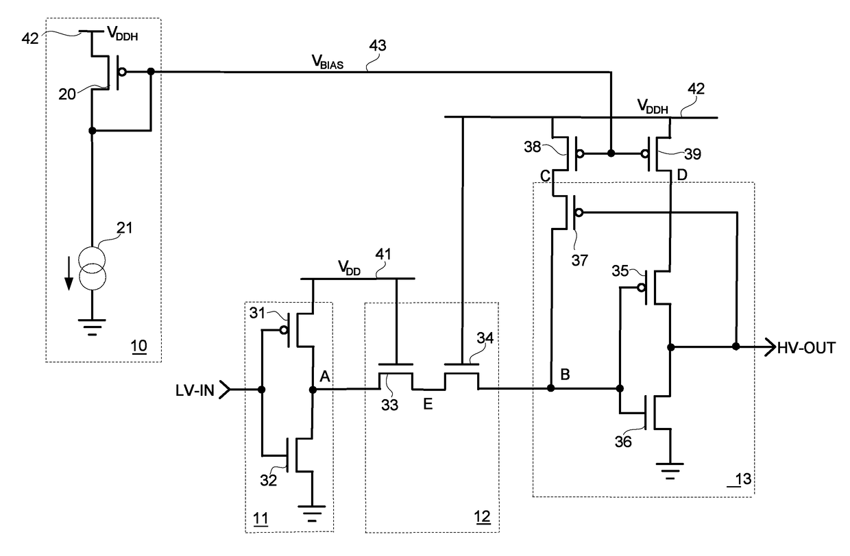
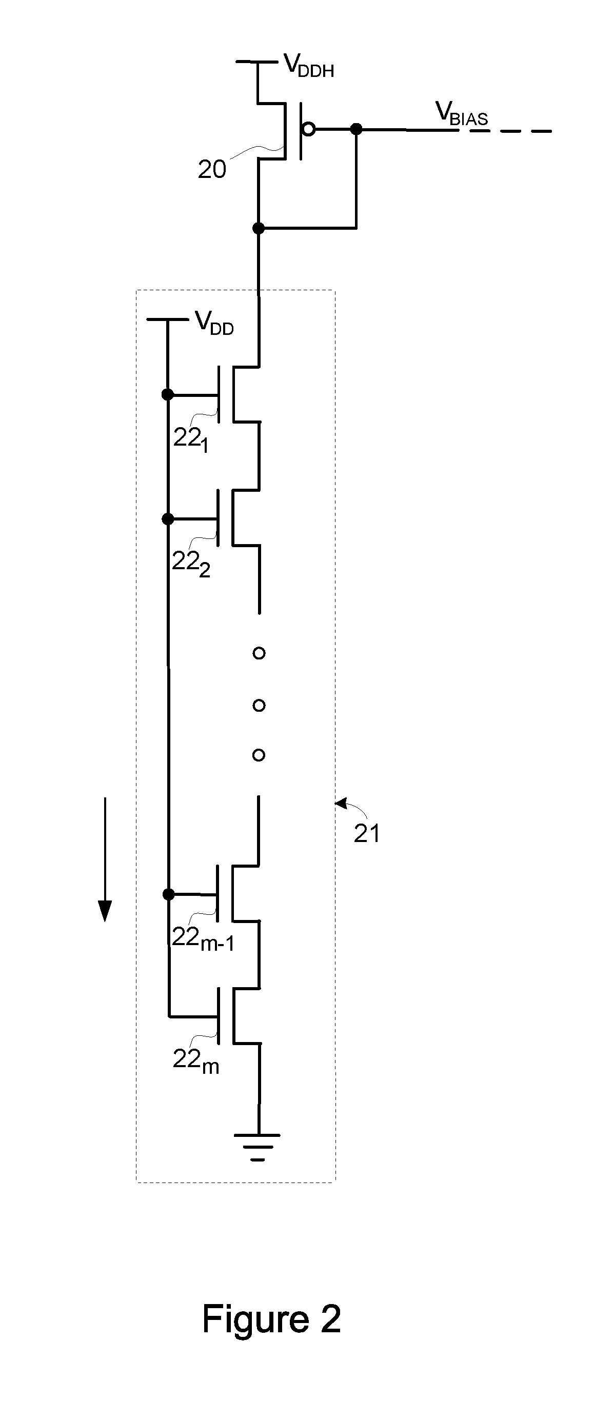
[0011]There are many applications for which the available power for an integrated circuit is very low. For example, an electronic device might harvest the power or energy from an external Radio-Frequency (RF) oscillating electric field, such as a passive RFID-tag (Radio Frequency IDentification tag). (An active RFID-tag has its own power supply, such as a battery.) The integrated circuit for the passive RFID-tag may contain a One-Time Programmable (OTP) memory and a logic controller block, each operating at different logic levels. The available power for the entire integrated circuit is very low, for example, 10 uW might be a typical value. The logic circuits in the integrated circuit must operate so as not to significantly disturb the power supply and a conventional voltage level shifter operating with the logic circuits could take so much current from the power supply that a single placement of the voltage level shifter circuit could collapse the supply when the attached logic cir...


PUM


Abstract

A low power voltage level shifter circuit in which current is limited through at least one of a plurality of CMOS logic circuits, one of which receives input signals within a first voltage level and is connected between a first upper and lower power supply, a second of which transmits shifted output signals within a second voltage level and is connected between a second upper and lower power supply. There is at least one current-limiting MOS transistor connected between at one of the CMOS logic circuits and one of its power supplies. Typically, there is at least one current-limiting MOS transistor between the second CMOS logic circuit which transmits the shifted output signals which have a larger range than that of the input signals. A second current through the at least one current-limiting MOS transistor mirrors a set current through a first MOS transistor so that power consumed by the CMOS logic circuit during switching is limited.

Description

BACKGROUND OF THE INVENTION[0001]This invention relates to a circuit which shifts a logic signal from one voltage level to another in an integrated circuit. In particular, the circuit shifts a logic signal from a low voltage supply magnitude to a higher voltage supply magnitude and is useful for systems with very low available power.[0002]This level shift function is needed whenever a logic gate output operating at one power supply voltage level drives the input of another logic gate which operates at a different power supply voltage level. An example of such a situation is in an integrated circuit having a One-Time-Programmable (OTP) memory where the address decoding logic, which may operate from a VDD=0.8V supply, needs to drive an OTP memory array decoder operating at 1.3V. That is, the address decoding logic circuits operate between 0V and 0.8V, and the memory array decoder circuits operate between 0V and 1.3V. This disparity in voltage levels requires a voltage level shifter ci...

Claims


Application Information

Patent Timeline
Patent Type & Authority Patents(United States)
IPC IPC(8): H03K19/094H03K19/0185H03K19/00
CPCH03K19/018521H03K19/0013
Inventor BILL, COLIN STEWART
Owner SYNOPSYS INC
Why Eureka
Try Eureka