Semiconductor device with an interconnection structure having interconnections with an interconnection density that decreases moving away from a cell semiconductor pattern

a technology of interconnection structure and interconnection density, which is applied in the direction of semiconductor devices, semiconductor/solid-state device details, electrical apparatus, etc., can solve the problems of process failure and device defects, increase the degree of integration, and limit the degree of integration of two-dimensional semiconductor devices

Active Publication Date: 2018-10-30
SAMSUNG ELECTRONICS CO LTD
View PDF17 Cites 15 Cited by
  • Summary
  • Abstract
  • Description
  • Claims
  • Application Information

AI Technical Summary

Problems solved by technology

For example, two-dimensional semiconductor devices including two-dimensionally arranged memory cells may require very expensive equipment to obtain fine-sized patterns which increase the degree of integration.
Accordingly, there is a limit to increasing the degree of integration of the two-dimensional semiconductor devices.
However, process failures and device defects may occur as pattern sizes of the three-dimensional semiconductor devices decrease.

Method used


Image

  • Semiconductor device with an interconnection structure having interconnections with an interconnection density that decreases moving away from a cell semiconductor pattern
  • Semiconductor device with an interconnection structure having interconnections with an interconnection density that decreases moving away from a cell semiconductor pattern
  • Semiconductor device with an interconnection structure having interconnections with an interconnection density that decreases moving away from a cell semiconductor pattern

Examples


Embodiment Construction

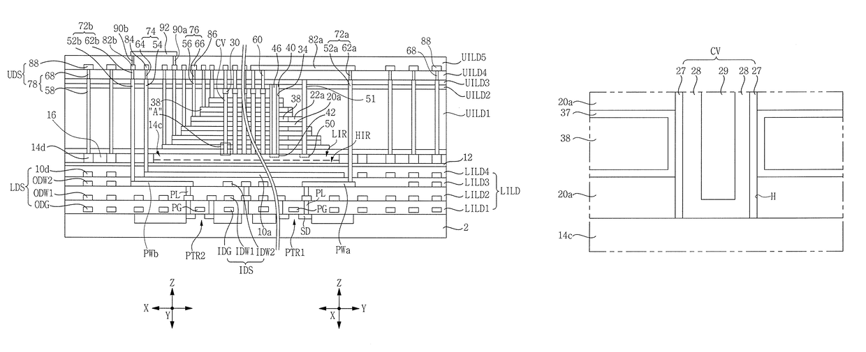
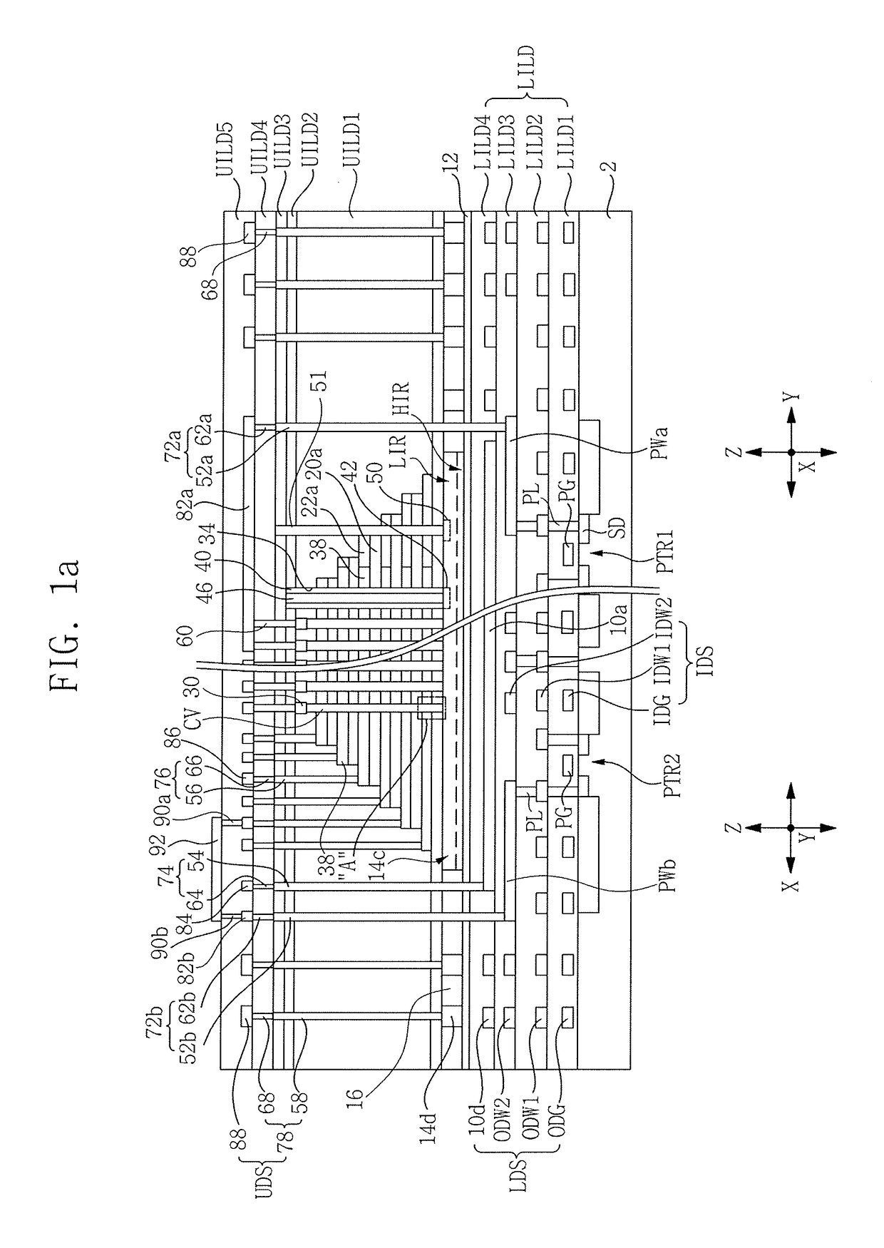
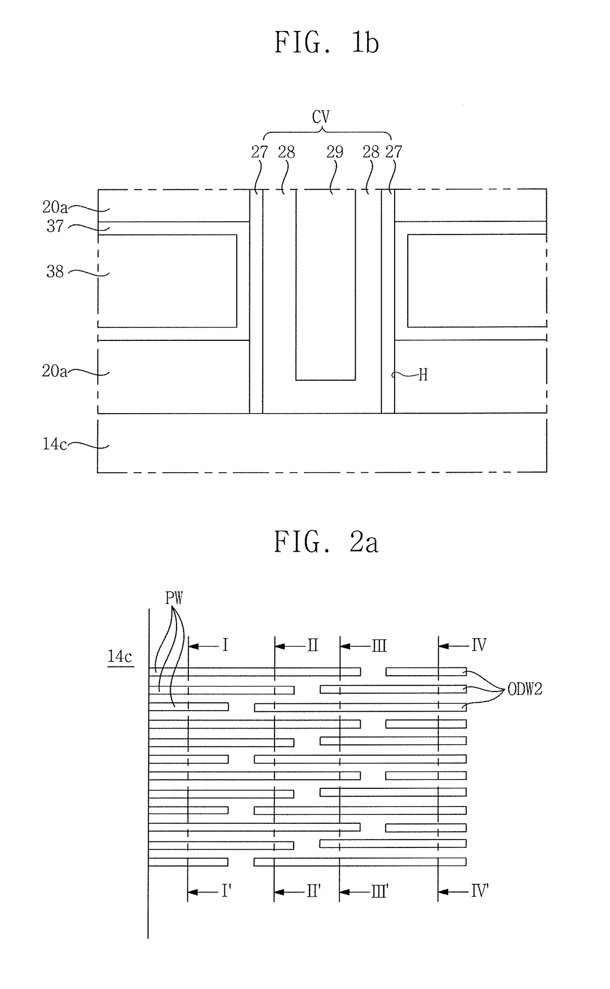
[0047]Hereinafter, exemplary embodiments of the inventive concept will be described in detail with reference to the accompanying drawings. The inventive concept may, however, be embodied in various different forms and should be construed as limited by the embodiments set forth herein. In the drawings, the sizes and relative sizes of layers and regions may be exaggerated for clarity. The same reference symbols may denote the same components throughout the specification.

[0048]Exemplary embodiments of the inventive concept are described herein with reference to cross-sectional views, plan views, and / or block diagrams that are schematic illustrations of idealized embodiments. As such, variations from the shapes of the illustrations as a result, for example, of manufacturing techniques and / or tolerances, are to be expected. Thus, the embodiments should not be construed as limited to the particular shapes of regions illustrated herein but are to include deviations in shapes that result, f...


PUM


Abstract

A semiconductor device includes a cell semiconductor pattern disposed on a semiconductor substrate. A semiconductor dummy pattern is disposed on the semiconductor substrate. The semiconductor dummy pattern is co-planar with the cell semiconductor pattern. A first circuit is disposed between the semiconductor substrate and the cell semiconductor pattern. A first interconnection structure is disposed between the semiconductor substrate and the cell semiconductor pattern. A first dummy structure is disposed between the semiconductor substrate and the cell semiconductor pattern. Part of the first dummy structure is co-planar with part of the first interconnection structure. A second dummy structure not overlapping the cell semiconductor pattern is disposed on the semiconductor substrate. Part of the second dummy structure is co-planar with part of the first interconnection structure. A conductive shielding pattern is disposed between the cell semiconductor pattern and the semiconductor substrate and above the first circuit and the first interconnection structure.

Description

CROSS-REFERENCE TO RELATED APPLICATION[0001]This application claims priority under 35 U.S.C. § 119 to Korean Patent Application No. 10-2014-0172283 filed on Dec. 3, 2014, the disclosure of which is incorporated by reference herein in its entirety.TECHNICAL FIELD[0002]Exemplary embodiments of the inventive concept relate to a semiconductor device, a method of fabricating the semiconductor device, and an electronic system employing the semiconductor device and the method.DESCRIPTION OF RELATED ART[0003]In semiconductor devices such as a flash memory, a degree of integration may be an important factor in determining price. For example, two-dimensional semiconductor devices including two-dimensionally arranged memory cells may require very expensive equipment to obtain fine-sized patterns which increase the degree of integration. Accordingly, there is a limit to increasing the degree of integration of the two-dimensional semiconductor devices. Three-dimensional semiconductor devices inc...

Claims


Application Information

Patent Timeline
Patent Type & Authority Patents(United States)
IPC IPC(8): H01L27/115H01L23/552H01L23/528H01L23/31H01L27/11573H01L27/06H01L27/11582
CPCH01L23/528H01L23/3192H01L23/552H01L27/0688H01L27/11573H01L2924/0002H01L27/11582H01L2924/00H01L23/522H10B43/40H10B43/27H10B53/50H10B53/40
Inventor YUN, JANG-GNYUN, JAESUNLIM, JOON-SUNG
Owner SAMSUNG ELECTRONICS CO LTD
Why Eureka
Try Eureka