Fabrication method of 3D high-density interconnected PoP plastic package device

A high-density interconnection and device technology, applied in semiconductor/solid-state device manufacturing, electrical solid-state devices, semiconductor devices, etc., to achieve the effects of feasibility, flexible packaging, and high yield

Inactive Publication Date: 2019-04-02
WUXI ZHONGWEI GAOKE ELECTRONICS
View PDF6 Cites 2 Cited by
  • Summary
  • Abstract
  • Description
  • Claims
  • Application Information

AI Technical Summary

Problems solved by technology

[0006] The purpose of the present invention is to solve the problem of vertical interconnection at the current module level. The present invention provides a method for preparing a 3D high-density interconnected PoP plastic packaging device. In the traditional PoP plastic packaging form, a conventional MCM substrate is used, and conven...

Method used


Image

  • Fabrication method of 3D high-density interconnected PoP plastic package device
  • Fabrication method of 3D high-density interconnected PoP plastic package device
  • Fabrication method of 3D high-density interconnected PoP plastic package device

Examples


Embodiment 1

[0043] Embodiment 1: One-sided interconnection PoP packaging form, including the following steps:

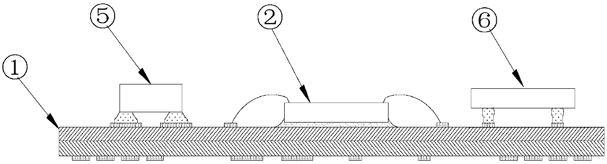
[0044] Such as Picture 1-1 As shown, step 1. Select a substrate 1, and perform flip chip 6 placement, SMT device 5 placement and other chip 2 placement bonding on the front of the substrate 1;

[0045] The substrate 1 in this embodiment 1 includes an MCM substrate.

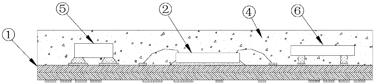
[0046] Such as Figure 1-2 As shown, step 2. Encapsulate the front of the substrate 1 with a plastic encapsulant 4 to complete the front encapsulation;

[0047] Such as Figure 1-3 As shown, step 3. On the back of the substrate 1, perform flip chip 6 mounting, SMT device 5 mounting, and copper pillar 3 pillar planting; in the process of pillar copper pillar 3, first apply solder paste on the substrate 1 at low temperature , using the reflow process after brushing the solder paste, and then reflow soldering the copper pillar 3;

[0048] Here, according to the specific application situation, other chips 2 can als...

Embodiment 2

[0053] Embodiment 2: The double-sided interconnection PoP encapsulation form includes the following steps:

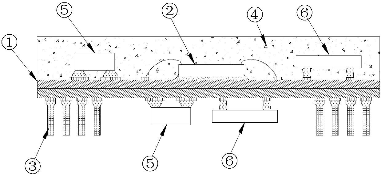
[0054] Such as diagram 2-1 As shown, step 1: chip 2 patch bonding and copper pillar 3 pillar planting are performed on the front of substrate 1; here, according to actual application conditions, flip chip 6 mounting, SMT device 5 mounting, etc. can be performed as appropriate;

[0055] Such as Figure 2-2 As shown, step 2: complete the plastic encapsulation on the front of the substrate 1;

[0056] Such as Figure 2-3 As shown, step 3: complete flip chip 6 placement, SMT device 5 placement and column planting process on the back of the substrate 1;

[0057] In the process of planting the copper pillar 3, first apply solder paste on the substrate 1 at low temperature, use the reflow process after brushing the solder paste, and then reflow solder the copper pillar 3;

[0058] Here, according to the specific application situation, other chips 2 can also be bonded;

...

Embodiment 3

[0063] Such as image 3 As shown, the 3D high-density interconnected PoP plastic packaged device stacked in the device includes the following steps:

[0064] Stack the single-sided interconnected PoP packaged device in real-time example 1 and the double-sided interconnected PoP packaged device in embodiment 2, and first tear off the protective film 8 on one side of the double-sided interconnected PoP packaged device to expose the 3 ends of the copper pillars , and then solder the solder ball 7 of the single-sided interconnected PoP packaged device to the exposed copper column end, thus completing the stacking of the single-sided interconnected PoP packaged device and the double-sided interconnected PoP packaged device;

[0065] The stacking form in Embodiment 3 is not limited to stacking two devices, nor is it limited to stacking single-sided and double-sided devices, but also stacking multiple single-sided / double-sided interconnected PoP packaged devices.

[0066] In the for...


PUM


Abstract

The invention belongs to the technical field of integrated circuit package, and relates to a fabrication method of a 3D high-density interconnected PoP plastic package device. The fabrication method comprises the steps of performing device surface-mounting on a front surface of an MCM substrate, and completing plastic package; completing SMT device surface-mounting and copper post surface-mountingin one time by a mode that tin paste is printed on a back surface of the substrate, and completing secondary plastic package of the back surface of the substrate; and thinning a plastic package bodyon the back surface of the substrate, exposing the copper post, and completing ball implantation at an exposure end of the copper post. The 3D high-density interconnected PoP plastic package device isin a way that on the basis of a PoP plastic device form, a conventional tin paste printing and copper post implantation process is used for substituting a vertical module through hole process, the process difficulty and cost can be reduced, the front-stage equipment investment is not needed, 3D stacking between devices is achieved, and meanwhile, the 3D direction interconnection density is further improved.

Description

technical field [0001] The invention relates to a method for manufacturing a POP plastic-encapsulated device, in particular to a method for manufacturing a 3D high-density interconnected PoP plastic-encapsulated device, and belongs to the technical field of integrated circuit packaging. Background technique [0002] Vertical interconnection is the development trend of high-density integrated packaging. Vertical interconnection is completed at the chip level through silicon via technology, and vertical interconnection is completed at the substrate level through the preparation process of built-in components. The corresponding vertical interconnection at the module level includes SiP and PoP. [0003] The chip-level 3D interconnection realized through TSV is not only complicated in the chip process, but also has high requirements on the placement accuracy and placement pressure of the placement equipment, so as to meet the multi-layer and high-density chip stacking interconnect...

Claims


Application Information

Patent Timeline
IPC IPC(8): H01L21/48H01L21/56H01L21/768
CPCH01L21/4853H01L21/4867H01L21/56H01L21/76895H01L2224/16225H01L2224/48091H01L2924/15332H01L2924/181H01L2924/19105H01L2924/00012H01L2924/00014
Inventor 杨婷李宗亚敖国军
Owner WUXI ZHONGWEI GAOKE ELECTRONICS
Why Eureka
Try Eureka