Wide dynamic range fluid sensor based on nanowire platform

a nanowire and fluid sensor technology, applied in the field of nanowire-based devices, can solve the problems of low dynamic range of high-sensitivity sensors, and achieve the effects of reducing processing complexity, saving cost, and saving further cos

Active Publication Date: 2018-11-13
KONINKLJIJKE PHILIPS NV
View PDF21 Cites 2 Cited by
  • Summary
  • Abstract
  • Description
  • Claims
  • Application Information

AI Technical Summary

Benefits of technology

[0018]The device can accordingly be made using conventional semiconductor materials and is therefore suitable for integration with CMOS-based circuits or with pre-existing lab-on-a-chip solutions using well developed fabrication techniques and requiring minimum adaptation of existing fabrication processes. The device may also advantageously be combined with other types of sensors such as temperature sensors, conductivity sensors etc. Additionally, by selecting different insulating materials for different nanowires, different substances can be detected simultaneously by one device. A further advantage of the present invention is that the compatibility with established processing methods means that sensor devices can be fabricated at a relatively low cost.
[0019]The degree of influence that the substance will have on the characteristic of the nanowire depends on compositional as well as structural parameters of the nanowire and additional layers. Each nanowire of said plurality of nanowires can comprises a surface area and a nanowire volume, wherein the ratio of the surface area and the volume is different for the different nanowires of said plurality of nanowires. The larger the ratio, the more sensitive the nanowire is to the presence of substance in its neighborhood and vice versa. The change of detection range, i.e., not necessarily an increase or decrease of the detection range, but simply a different range, comes with a change of the ratio. The nanowire may have a detection surface exposed at its side where the sample compartment extends. The detection surface can be arranged for the detecting of the presence of the substance.
[0020]To vary the ratio among the different nanowires of the plurality of nanowires, the length, width or height (thickness) of the nanowire can be used. Preferably then the length or the width are varied while the thickness (perpendicular to substrate layer extension) is kept constant. If the plurality of nanowires is arranged in a planar substrate, then the plurality of different dimensions of the nanowires may be defined in one and the same patterning (masks) step again saving further cost. Also, in many regular substrates, the layer wherein the nanowires are made is a uniform thickness deposited layer of semiconductor such as silicon. Hence standard substrates can be used and etch steps to vary thickness of that layer are not needed thus reducing processing complexity and saving cost. It is preferred that the nanowire width is varied while also the length is kept constant for the plurality of nanowires. The width of nanowires preferably is in the range 8 nm to 1 micrometer. The lower range is in practice limited to smallest feature sizes that can be patterned using lithography or imprint techniques. A preferred range is 50 nm to 500 nm. A more preferred range is 10 nm to 500 nm. Within these ranges there can be nanowires with widths of 10, 15, 20, 25, 30, 50, 100, 200 300, and 400 nm or any combination. This gives nanowires that due to their length still give resistances that can be used in regular IC structures. (Note that the cross section of the nanowire determines its resistance). Lengths of nanowires may be in between 1 to 10 micrometer. They can be lower than 2 micrometer, lower than 1 micrometer, or lower than 500 nm.
[0021]Alternatively or additionally, to the dimensional variation between the nanowires of the plurality of nanowires, the thickness of the insulating material and the choice of insulator material covering the nanowire can be changed to implement variations of detection range. Influence of the substance to the characteristics of the nanowire can be through capacitive coupling. Thus, an increase of insulator thickness gives a smaller coupling and less sensitivity and vice versa. Also, variation of material to larger dielectric constant will give increase coupling and increased sensitivity and vice versa. Again adjustment of these parameters comes with different detection range. As the dielectric constant is largely determined by the insulating material which is generally compatible with the substrate materials and processing, the thickness of the layer is the preferred parameter to vary across the nanowires of the plurality of nanowires. The thickness is preferably between 1 nm and 10 nm to give a good sensitivity. If increased sensitivity is needed, the thickness is in the range 1 to 4 nm, most preferably 3 nm. If increased reliability with regard to electrical insulation of the insulating material layer is needed, the thickness preferably is in the range of 6 to 10 nm, most preferably 7 nm. A thickness of 5 nm gives a good compromise between sensitivity and reliability.
[0022]As an example, a nanowire with a smaller cross sectional area and a thinner insulating layer will be influenced more by a substance molecule than a wire with a larger area and a thicker insulating layer. Such influence can be via capacitive or inductive changes of the nanowire between situation with substance or without substance.
[0023]The device of the invention may be a pH detection device. The insulting layer over the nanowire can be Silicon oxide for this purpose. The surface of silicon oxide generally has Si—OH groups of which the H+ (substance) is reversibly exchangeable with the sample fluid (preferably comprising or consisting of water for good definition of pH). Hence the charge of a surface layer of the silicon oxide (Si—O−) on depends on the pH of the fluid, i.e., high pH reduced bound H+ and large O− surface charge and low pH, all groups converted to Si—OH and no charge on the surface. The charge determines the conductivity of the nanowire and that can be used as a characteristic of the nanowire to measure.

Problems solved by technology

It is a problem of the known detector devices that a high sensitivity sensor comes with a low dynamic range.

Method used


Image

  • Wide dynamic range fluid sensor based on nanowire platform
  • Wide dynamic range fluid sensor based on nanowire platform
  • Wide dynamic range fluid sensor based on nanowire platform

Examples


Embodiment Construction

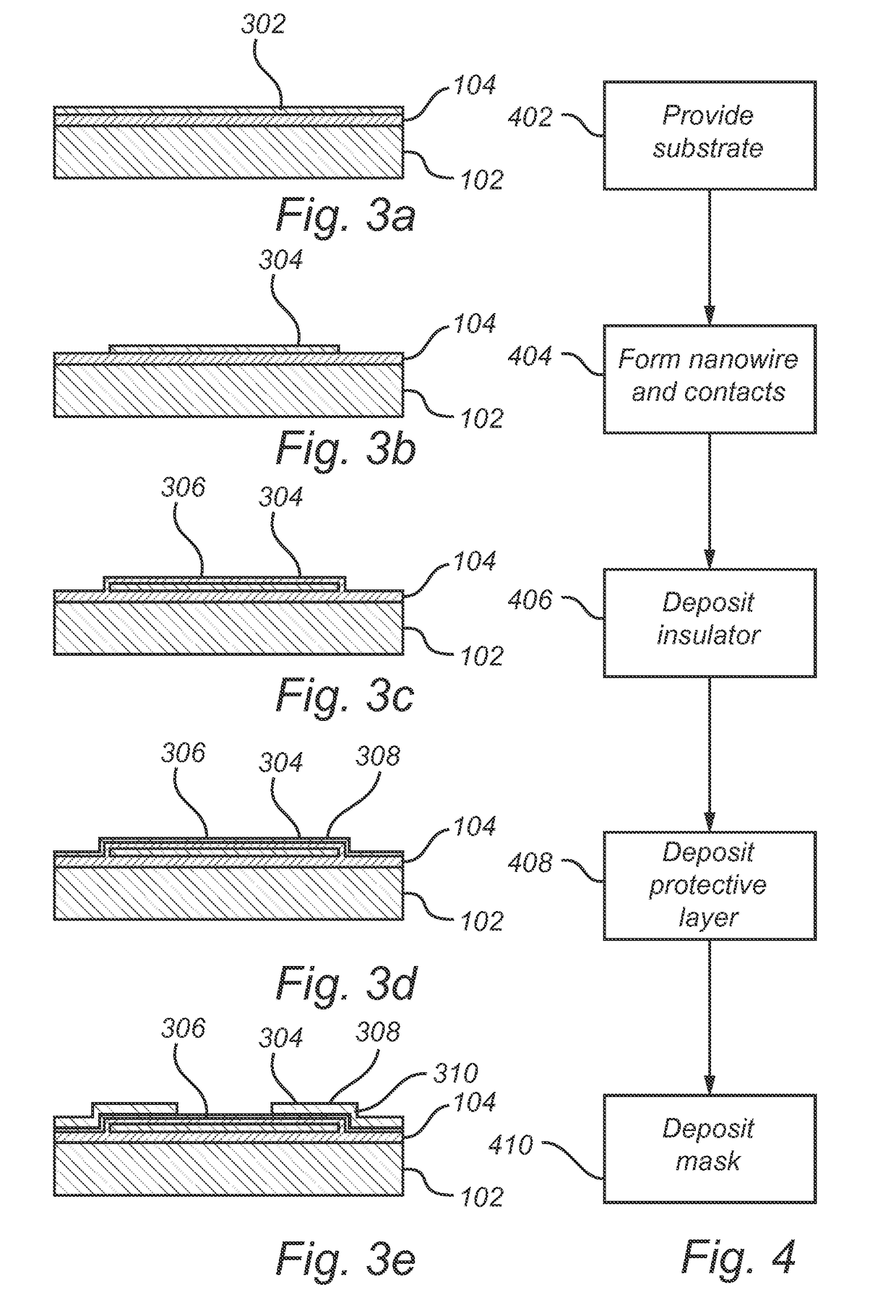
[0051]In the present detailed description, various embodiments of a device according to the present invention are mainly discussed with reference to a device comprising silicon nanowires based on an SOI (silicon-on-insulator) substrate. It should be noted that this by no means limits the scope of the present invention which is equally applicable to devices comprising nanowires based on other semiconductor materials which also may be formed on other types of substrates.

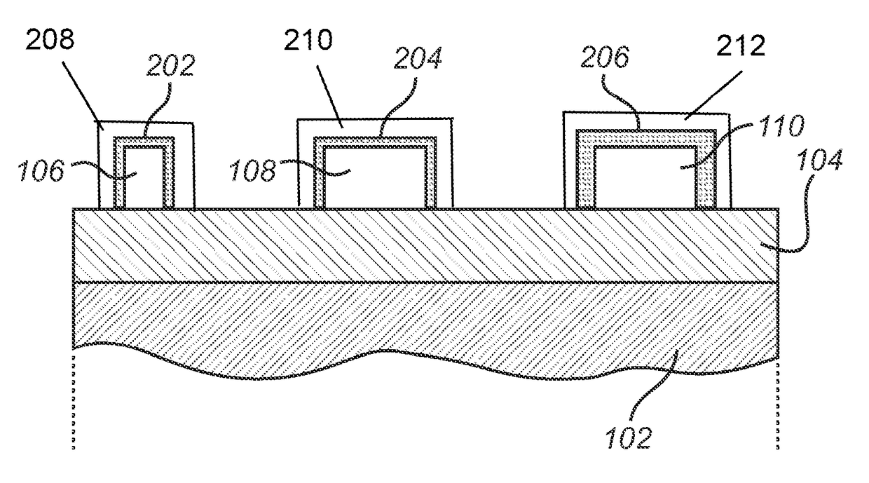
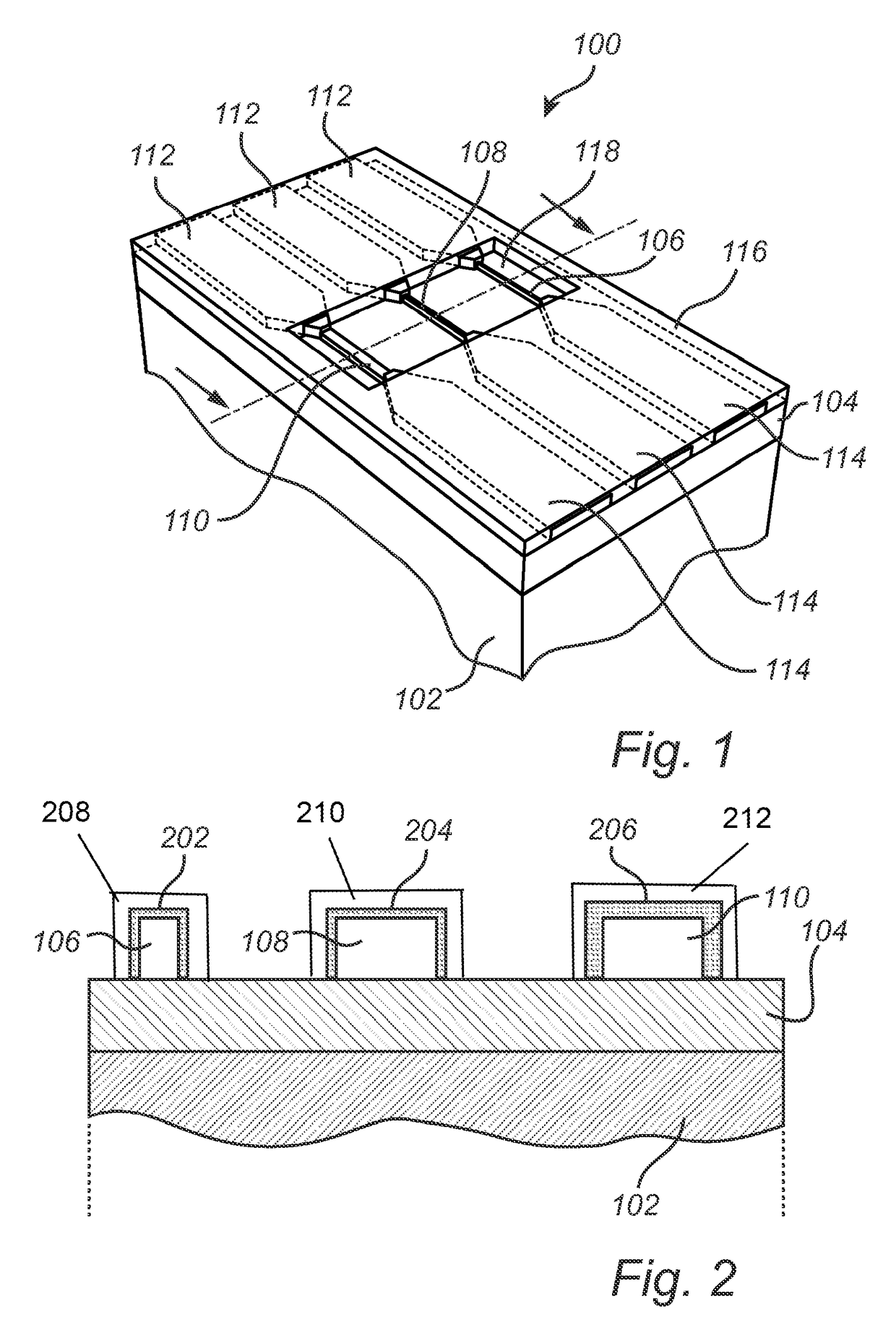
[0052]FIG. 1 schematically illustrates a device 100 according to an embodiment of the invention. It should be noted that the device in FIG. is not drawn to scale and that the purpose of the drawing merely is to illustrate the general concepts of the invention.

[0053]The device 100 comprises a substrate 102, an insulating layer 104 arranged on the substrate 102, three nanowires 106, 108, 110 arranged in parallel are formed in the top silicon layer of an SOI-substrate. There is further illustrated conductive contacting st...


PUM

PropertyMeasurementUnit
widthaaaaaaaaaa
widthsaaaaaaaaaa
widthsaaaaaaaaaa

Abstract

A device for detecting a concentration of a substance in a fluid sample includes a substrate; an insulating layer arranged on the substrate; and a plurality of individually electrically addressable semiconducting nanowires arranged on the insulating layer. Each one of the plurality of nanowires is covered by an insulating material and arranged for sensing of the substance through an electrical characteristic of the nanowire. The device further includes a sample compartment for providing the fluid sample in contact with each of the plurality of nanowires. For each of the plurality of nanowires, at least one of the cross sectional dimension, the insulator thickness and the type of insulating material is selected such that each of the nanowires has a different detection range, and such that the dynamic range of the device is higher than the dynamic range of each of the individual nanowires.

Description

[0001]This application is the U.S. National Phase application under 35 U.S.C. § 371 of International Application No. PCT / IB2013 / 059160, filed on Oct. 7, 2013, which claims the benefit of U.S. Provisional Application No. 61 / 714,418 filed on Oct. 16, 2012. These applications are hereby incorporated by reference herein.FIELD OF THE INVENTION[0002]The present invention relates to a device for detecting a concentration of a substance in a fluid. In particular, the present invention relates to a nanowire-based device.BACKGROUND OF THE INVENTION[0003]Sensors for detection of biological substances based on nanoscale field-effect transistors, such as for example silicon nanowire FETs and carbon nanotubes with properly functionalized surfaces, have enormous potential for very sensitive detection of minute (down to femtomolar) concentrations of biomolecules such as proteins and DNA. In addition, when proper interface layers are applied through functionalization of the surface in contact with t...

Claims


Application Information

Patent Timeline
Patent Type & Authority Patents(United States)
IPC IPC(8): G01N27/00G01N27/414G01N33/00H01L29/06
CPCG01N27/4146H01L29/0673G01N33/0031G01N27/414
Inventor KLOOTWIJK, JOHAN HENDRIKMULDER, MARCEL
Owner KONINKLJIJKE PHILIPS NV
Why Eureka
Try Eureka