

Process of forming a photoactive layer of a perovskite photoactive device
a photoactive device and photoactive layer technology, applied in the direction of light-sensitive devices, solid-state devices, electrolytic capacitors, etc., can solve the problem of difficult fabrication of continuous film layers comprising uniform crystal structures, and achieve the effect of improving the cell's sunlight to electrical energy conversion efficiency, broader spectral response and high efficiency
- Summary
- Abstract
- Description
- Claims
- Application Information
AI Technical Summary
Benefits of technology
Problems solved by technology
Method used
Image

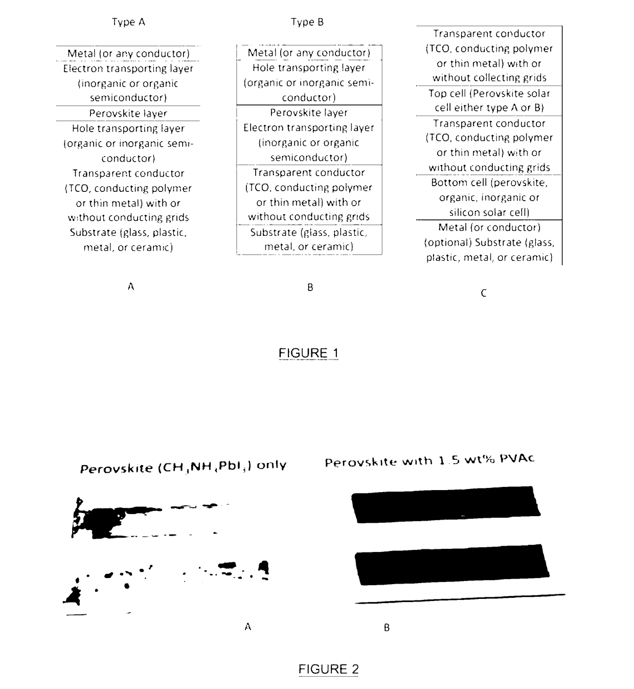
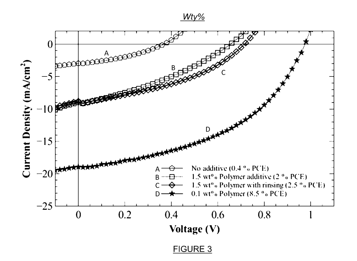
Examples
example 1
mer Additive
(1) Material Preparation.
Preparation of ZnO Precursor:
[0124]A ZnO precursor was prepared by dissolving zinc acetate dihydrate (Zn(CH3COO)2·2H2O, Aldrich, 99.9%, 1 g) and ethanolamine (NH2CH2CH2OH, Aldrich, 99.5%, 0.28 g) in 2-methoxyethanol (CH3OCH2CH2OH, Aldrich, 99.8%, 10 mL) under vigorous stirring for 12 h.
Preparation of ZnO Nanoparticle:
[0125]ZnO nanoparticles were synthesized from zinc acetate dehydrate and sodium hydroxide (NaOH). The zinc acetate solution was prepared by dissolving zinc acetate dihydrate (0.230 g) in ethanol (15 mL) at 75° C. and the NaOH solution was prepared by dissolving NaOH (0.1 g) in ethanol (5 mL). The NaOH solution was added dropwise to the zinc acetate solution at RT under vigorous stirring. Subsequently, the transparent suspension showed green emission under excitation by an UV lamp. The transparent suspension of nanoparticles was purified by repeated precipitation with heptane, centrifuging and redispersion in EtOH. The washed suspensi...
PUM
| Property | Measurement | Unit |
|---|---|---|
| thickness | aaaaa | aaaaa |
| wt % | aaaaa | aaaaa |
| thickness | aaaaa | aaaaa |
Abstract
Description
Claims
Application Information