Integrated circuit structure incorporating stacked field effect transistors

a technology of integrated circuits and transistors, applied in the direction of semiconductor devices, semiconductor/solid-state device details, electrical apparatus, etc., can solve the problems of limiting area savings, complex supply of power and/or signal connections to the source/drain region of the lower gaafet, and corresponding increase in short channel effects

Active Publication Date: 2019-01-29
GLOBALFOUNDRIES US INC
View PDF22 Cites 24 Cited by
  • Summary
  • Abstract
  • Description
  • Claims
  • Application Information

AI Technical Summary

Problems solved by technology

For example, size scaling of planar field effect transistors (FETs) resulted in the development of planar FETs with relatively short channel lengths but, unfortunately, the smaller channel lengths resulted in a corresponding increase in short channel effects.
Unfortunately, while stacked pairs of N-type and P-type GAAFETs consume less chip area than side-by-side pairs of N-type and P-type GAAFETs, providing the necessary power and / or signal connections to the source / drain regions of the lower GAAFETs can be complex and may limit the area savings.

Method used


Image

  • Integrated circuit structure incorporating stacked field effect transistors
  • Integrated circuit structure incorporating stacked field effect transistors
  • Integrated circuit structure incorporating stacked field effect transistors

Examples


Embodiment Construction

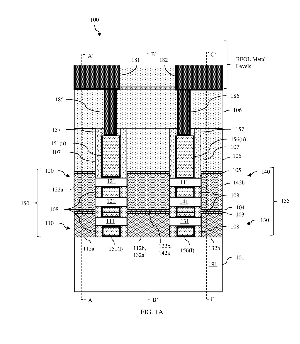
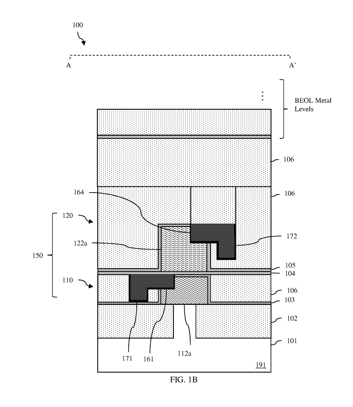
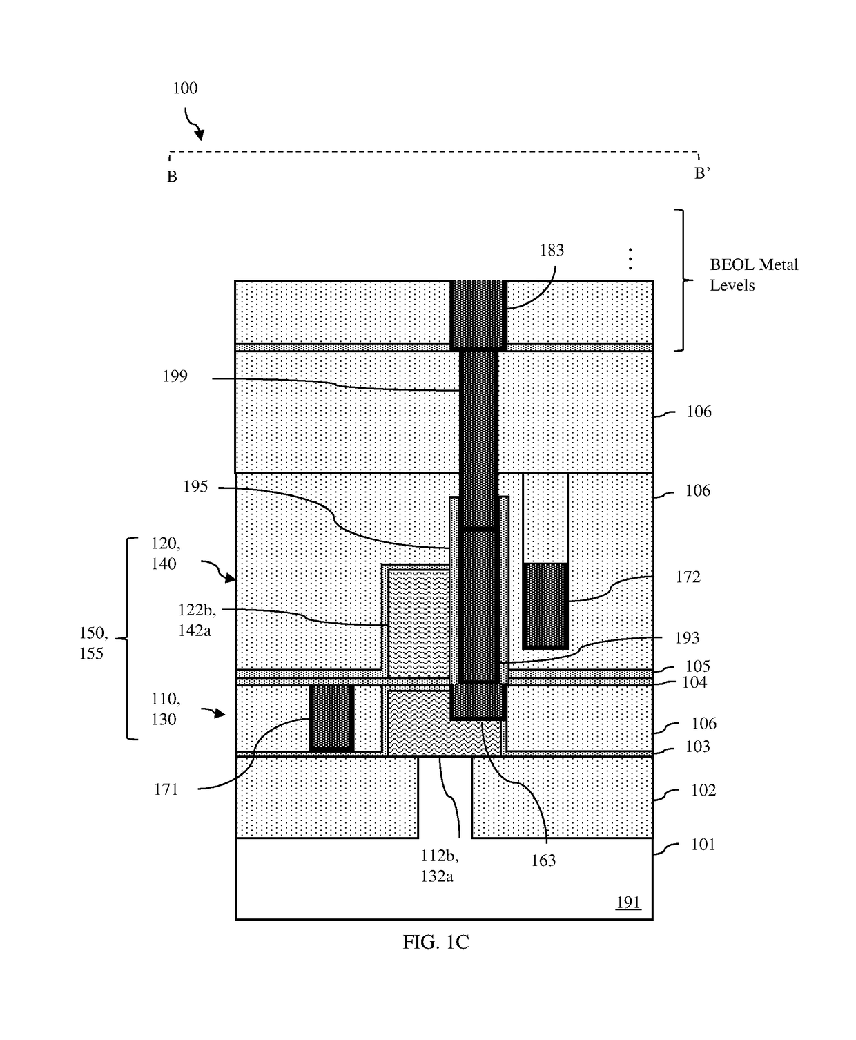
[0028]As mentioned above, a conventional layout with multiple gate-all-around field effect transistors (GAAFETs) will typically have a row of N-type GAAFETs on one-side, a corresponding row of P-type GAAFETs on the opposite side, and shared gates that extend laterally across and wrap around the channel regions of side-by-side pairs of N-type and P-type GAAFETs. Contrarily, a layout with multiple stacked pairs of GAAFETs will have P-type GAAFETs on one-level, N-type GAAFETs on an adjacent level (i.e., above or below) and, shared gates, where each shared gate extends vertically across and wraps around the channel regions of a stacked pair of N-type and P-type GAAFETs. In this case, the source / drain regions of the lower GAAFET will be electrically isolated from the source / drain regions of the upper GAAFET by dielectric layers. Unfortunately, while stacked pairs of N-type and P-type GAAFETs consume less chip area than side-by-side pairs of N-type and P-type GAAFETs, providing the necess...


PUM


Abstract

Disclosed are integrated circuit (IC) structure embodiments that incorporate a stacked pair of field effect transistors (FETs) (e.g., gate-all-around FETs) and metal components that enable power and / or signal connections to source / drain regions of those FETs. Specifically, the IC includes a first FET and a second FET stacked on and sharing a gate with the first FET. The metal components include an embedded contact in a source / drain region of the first FET and connected to a wire (e.g., a power or signal wire). The wire can be a front end of the line (FEOL) wire positioned laterally adjacent to the source / drain region and the embedded contact can extend laterally from the source / drain region to the FEOL wire. Alternatively, the wire can be a back end of the line (BEOL) wire and an insulated contact can extend vertically from the embedded contact through the second FET to the BEOL wire.

Description

BACKGROUNDField of the Invention[0001]The present invention relates to integrated circuit (IC) structures and, more particularly, to embodiments of an IC structure that incorporates stacked field effect transistors (FETs), such as stacked gate-all-around field effect transistors (GAAFETs), and various metal components that enable power and / or signal connections to the source / drain regions of the FETs.Description of Related Art[0002]Integrated circuit (IC) design decisions are often driven by device scalability, device density, manufacturing efficiency and costs. For example, size scaling of planar field effect transistors (FETs) resulted in the development of planar FETs with relatively short channel lengths but, unfortunately, the smaller channel lengths resulted in a corresponding increase in short channel effects.[0003]In response, fin-type FETs (FINFETs) were developed. A FINFET is a non-planar FET that incorporates a semiconductor fin (i.e., an elongated, relatively tall and th...

Claims


Application Information

Patent Timeline
Patent Type & Authority Patents(United States)
IPC IPC(8): H01L29/00H01L23/50H01L25/07H01L29/417H01L21/8234
CPCH01L23/50H01L25/074H01L29/41791H01L21/823475H01L2924/14H01L23/485H01L29/0673H01L29/42392H01L29/78696B82Y10/00H01L29/41725H01L29/42376H01L29/66439H01L29/775H01L29/0692H01L27/0688H01L27/088H01L27/092H01L21/823871H01L21/8221H01L21/743H01L23/535H01L21/823842H01L29/66545H01L23/52H01L29/785
Inventor CHANEMOUGAME, DANIELLIEBMANN, LARSXIE, RUILONG
Owner GLOBALFOUNDRIES US INC
Why Eureka
Try Eureka