Method for integration of magnetic random access memories with improved lithographic alignment to magnetic tunnel junctions

a random access memory and magnetic tunnel junction technology, applied in multicolor photographic processing, instruments, photomechanical equipment, etc., can solve the problems of poor alignment, inability to see the alignment marks of the metal level therein, and peeling of a plurality, so as to improve the alignment to the ja lithographic patterning level

Inactive Publication Date: 2010-11-02
GLOBALFOUNDRIES US INC
View PDF9 Cites 19 Cited by
  • Summary
  • Abstract
  • Description
  • Claims
  • Application Information

AI Technical Summary

Benefits of technology

[0030]It is an object of this invention to improve alignment to the JA lithographic patterning level by eliminating the problems associated with the peeling of JA alignment marks.
[0031]This invention allows for a scheme to circumvent the problem of peeling or roughness and hence to provide a satisfactorily reliable form of alignment marking of MJT devices formed during JA lithographic processing.
[0032]In accordance with this invention, techniques are provided for aligning subsequent upper lithographic levels to MTJ structures. More specifically, the present invention provides techniques for creating enhanced alignment marks at the level of the MTJ structures that can be invoked while aligning subsequent upper levels.

Problems solved by technology

Unfortunately, there could be a problem with peeling of a plurality of JA alignment mark features 148A, which are shown in FIG. 1C, as metal stacks tend to peel and delaminate after patterning when cast into elongated shapes such as long lines needed in the alignment mark features 148A.
An engineering challenge in inserting MRAM devices during Back End Of Line (BEOL) semiconductor processing of Complementary Metal Oxide Semiconductor (CMOS) integration, is encountered in attempting to provide lithographic alignment of MTJ structures to the metal level therebelow.
However, when a MTJ metal stack is opaque there is the problem that the alignment marks of the metal level therebelow are not visible.
The variability introduced into the scattering of the laser light used by steppers to sense the alignment marks could contribute to poor alignment.

Method used


Image

  • Method for integration of magnetic random access memories with improved lithographic alignment to magnetic tunnel junctions
  • Method for integration of magnetic random access memories with improved lithographic alignment to magnetic tunnel junctions
  • Method for integration of magnetic random access memories with improved lithographic alignment to magnetic tunnel junctions

Examples


Embodiment Construction

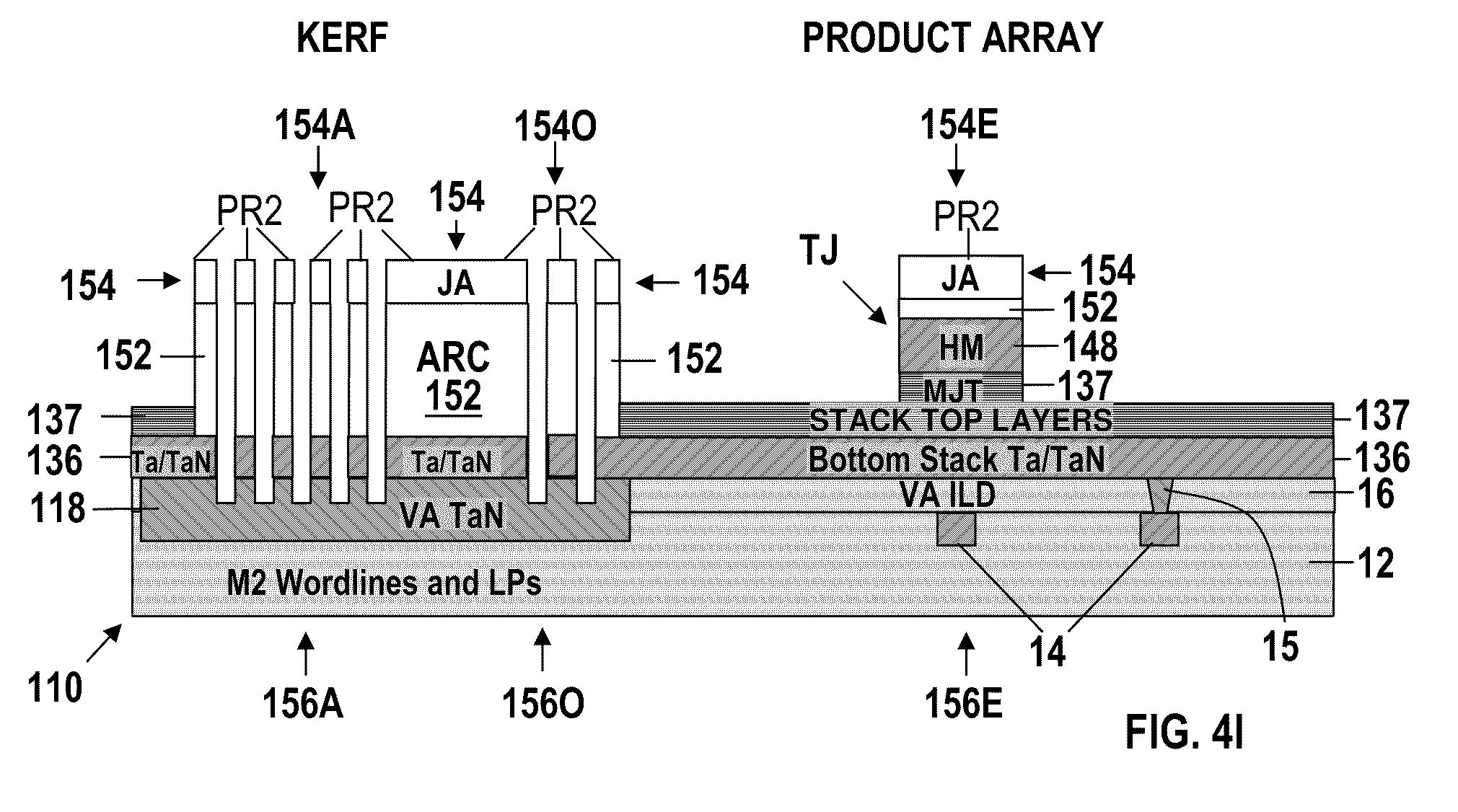
[0047]FIGS. 4A-4L are sectional elevational views of an MRAM device 110 in the process of being manufactured in accordance with the method of this invention. In accordance with this invention, techniques are provided for aligning subsequent upper lithographic levels to MTJ structures. More specifically, the present invention provides techniques for creating enhanced alignment marks at the level of the MTJ structures that can be invoked while aligning subsequent upper levels.

Step A

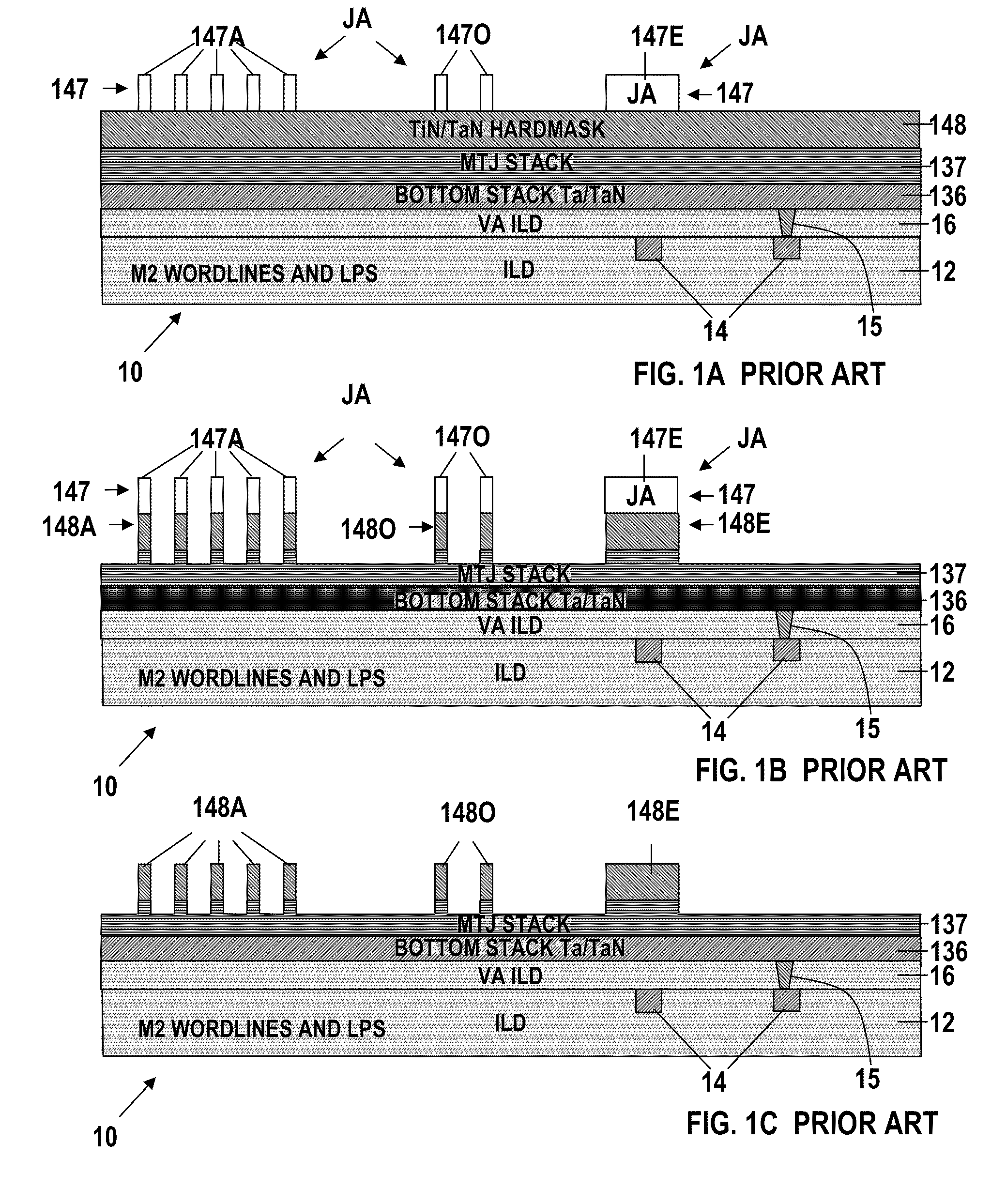
[0048]FIG. 4A shows a sectional elevational view of an MRAM device 110 in an early stage of manufacture. The device 110 comprises a lower Inter Level Dielectric (ILD) substrate layer 12 in the upper surface of which, electric conductors 14 have been formed for providing electrical interconnections between features within the device 110. A via level (VA) ILD layer 16 composed of a refractory material, e.g. a bilayer of tantalum over tantalum nitride, has been formed on the top surface of the lower ILD substr...


PUM


Abstract

A magnetic memory device including a Magnetic Tunnel Junction (MTJ) device comprises a substrate and Front End of Line (FEOL) circuitry. A Via level (VA) InterLayer Dielectric (ILD) layer, a bottom conductor layer, and an MTJ device formed over the top surface of the VA ILD layer are formed over a portion of the substrate. An alignment region including alignment marks extends through the bottom conductor layer and extends down into the device below the top surface of the VA ILD layers is juxtaposed with the MJT device.

Description

BACKGROUND OF THE INVENTION[0001]The present invention relates to semiconductor memory devices in the form of Magnetic Tunnel Junction (MTJ) cells of the type used as storage elements in Magnetic Random Access Memory (MRAM) devices and more particularly to alignment structures formed therein and methods of manufacture thereof.[0002]MRAM devices are based on arrays of MTJ cells. An MTJ cell is a MagnetoResistive (MR) device also known as a Tunnel Junction (TJ) which consists inter alia of two magnetic films; a Pinned Layer (PL) and a Free Layer (FL) separated by a tunnel barrier layer. The PL of the MTJ cell has an irreversible direction of magnetization as it is pinned or fixed by a variety of techniques. In contrast, the magnetization of the FL of the MTJ cell is programmable to be either parallel or anti-parallel to that of the PL during a “WRITE” operation in which data is stored in a memory cell. A thin tunnel barrier which is typically composed of aluminum oxide (Al2O3) is sand...

Claims


Application Information

Patent Timeline
Patent Type & Authority Patents(United States)
IPC IPC(8): H01L21/76H01L21/00
CPCH01L23/544H01L27/222H01L43/12H01L2223/54453H01L2924/0002Y10S438/975H01L2924/00H10B61/00H10N50/01
Inventor KANAKASABAPATHY, SIVANANDA K.ASSEFA, SOLOMON
Owner GLOBALFOUNDRIES US INC
Why Eureka
Try Eureka