Chip resistor and method for manufacturing same

a technology of resistor and chip, which is applied in the manufacture of resistor chips, resistor details, resistive material coatings, etc., can solve the problems of conduction failure or disconnection, sulfurization of the pair of electrodes, etc., and achieve high sulfurization resistance of electrodes. , the effect of high accuracy

Active Publication Date: 2019-03-05
KOA CORP
View PDF10 Cites 2 Cited by
  • Summary
  • Abstract
  • Description
  • Claims
  • Application Information

AI Technical Summary

Benefits of technology

[0017]According to the invention, it is possible to provide a chip resistor whose resistance value can be adjusted with high accuracy while maintaining high sulfurization resistance of electrodes of the chip resistor even in the case where the resistance value of the chip resistor is low, and a method for manufacturing this chip resistor.

Problems solved by technology

As to the chip resistor, sulfurization of the pair of electrodes has been regarded as a problem.
It is because sulfurization of the pair of electrodes may likely lead to conduction failure or disconnection.

Method used


Image

  • Chip resistor and method for manufacturing same
  • Chip resistor and method for manufacturing same
  • Chip resistor and method for manufacturing same

Examples


Embodiment Construction

[0024]A chip resistor and a method for manufacturing the same according to an embodiment of the invention will be described below with reference to the drawings.

(Configuration of Chip Resistor According to Embodiment of the Invention)

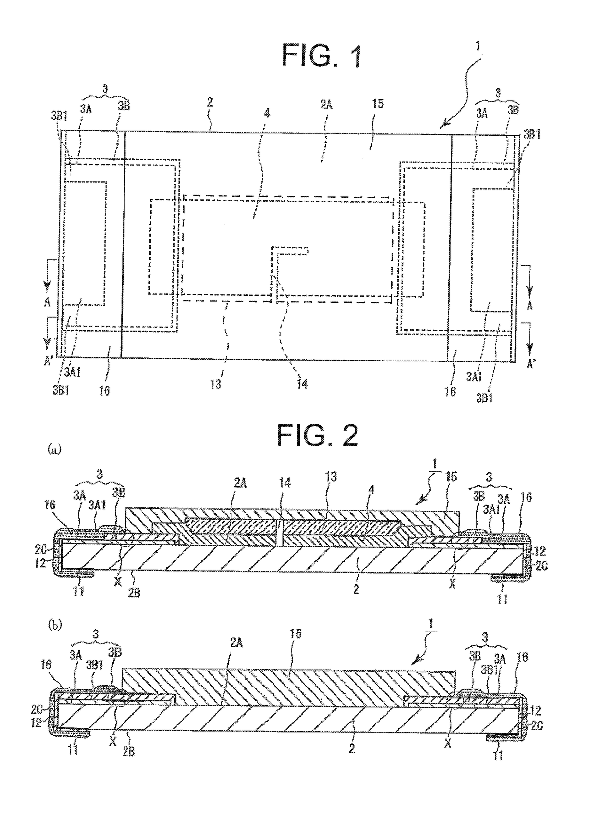
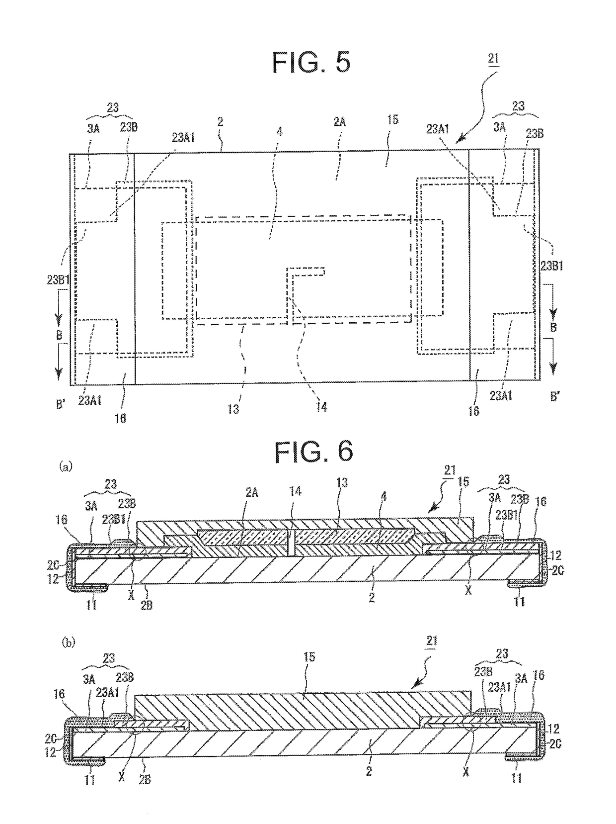
[0025]FIG. 1 is a plan view of a chip resistor according to an embodiment of the invention. FIG. 2 (a) is a sectional view taken along the line A-A of FIG. 1. FIG. 2(b) is a sectional view taken along the line A′-A′ of FIG. 1. The chip resistor 1 has an insulating substrate 2, a pair of electrodes 3, 3, a resistor substance 4, and an insulating film (an overcoat 15 which will be described later). The pair of electrodes 3, 3 are formed on an upper surface 2A of the insulating substrate 2. The resistor substance 4 containing ruthenium tetroxide as a main component is formed to make contact with both of the pair of electrodes 3, 3. The insulating film covers the resistor substance 4 and covers parts of the pair of electrodes 3, 3.

[0026]Each of the pair of ...


PUM


Abstract

A chip resistor including an insulating film covering a resistor making contact with a pair of electrodes formed on an upper surface of an insulating substrate and a method for manufacturing same are provided. Both electrodes include a main electrode layer that contains silver as a main metal component an 10 weight % or more of palladium as another metal component, and an auxiliary electrode layer lower in specific resistance than the main electrode layer, a laminate part where the auxiliary electrode layer and the main electrode layer are laminated in order on a single surface of the insulating substrate; and an exposed part of the auxiliary electrode layer where a part of the auxiliary electrode layer is not covered with the main electrode layer on a far side from the resistor, and part that extend from a near side to the far side with respect to the resistor.

Description

TECHNICAL FIELD[0001]The present invention relates to a chip resistor and a method for manufacturing the same.BACKGROUND ART[0002]A chip resistor has a pair of electrodes, a resistor substance, and an insulating film. The pair of electrodes containing silver as a main component are formed on a single surface of an insulating substrate. The resistor substance is formed on the single surface of the insulating substrate to make contact with both of the pair of electrodes. The insulating film covers the resistor substance while keeping parts of the pair of electrodes exposed. As to the chip resistor, sulfurization of the pair of electrodes has been regarded as a problem. It is because sulfurization of the pair of electrodes may likely lead to conduction failure or disconnection.[0003]To solve this problem, for example, there has been proposed a technique in which a metal material containing silver and palladium is used as the metal material of the pair of electrodes to thereby suppress ...

Claims


Application Information

Patent Timeline
Patent Type & Authority Patents(United States)
IPC IPC(8): H01C1/148H01C1/012H01C7/00H01C17/06H01C17/242H01C1/12H01C1/14H01C17/00
CPCH01C1/148H01C1/012H01C1/12H01C17/242H01C7/00H01C17/006H01C17/06H01C1/14
Inventor MATSUMOTO, KENTARO
Owner KOA CORP
Why Eureka
Try Eureka