Semiconductor device

a technology of semiconductors and capacitors, applied in the direction of galvano-magnetic devices, instruments, magnetic measurements, etc., can solve the problem that the offset voltage cannot be eliminated completely, and achieve the effect of effectively eliminating the offset voltag

Active Publication Date: 2019-04-16
ABLIC INC
View PDF8 Cites 0 Cited by
  • Summary
  • Abstract
  • Description
  • Claims
  • Application Information

AI Technical Summary

Benefits of technology

[0011]It is therefore an object of the present invention to provide a semiconductor device that includes a vertical Hall element capable of effectively removing an offset voltage.
[0014]This configuration keeps the shapes of current paths substantially the same or symmetrical despite the switch of electrodes that are used as control current supply electrodes by spinning current, that is, despite a change of location where a current flows or a change of direction in which a current flows between the same two control current supply electrodes. The offset voltage can therefore be eliminated effectively by spinning current.

Problems solved by technology

However, the offset voltage is not considered in Japanese Patent Publication No.
The offset voltage cannot be eliminated completely as a result.

Method used


Image

  • Semiconductor device
  • Semiconductor device
  • Semiconductor device

Examples


first embodiment

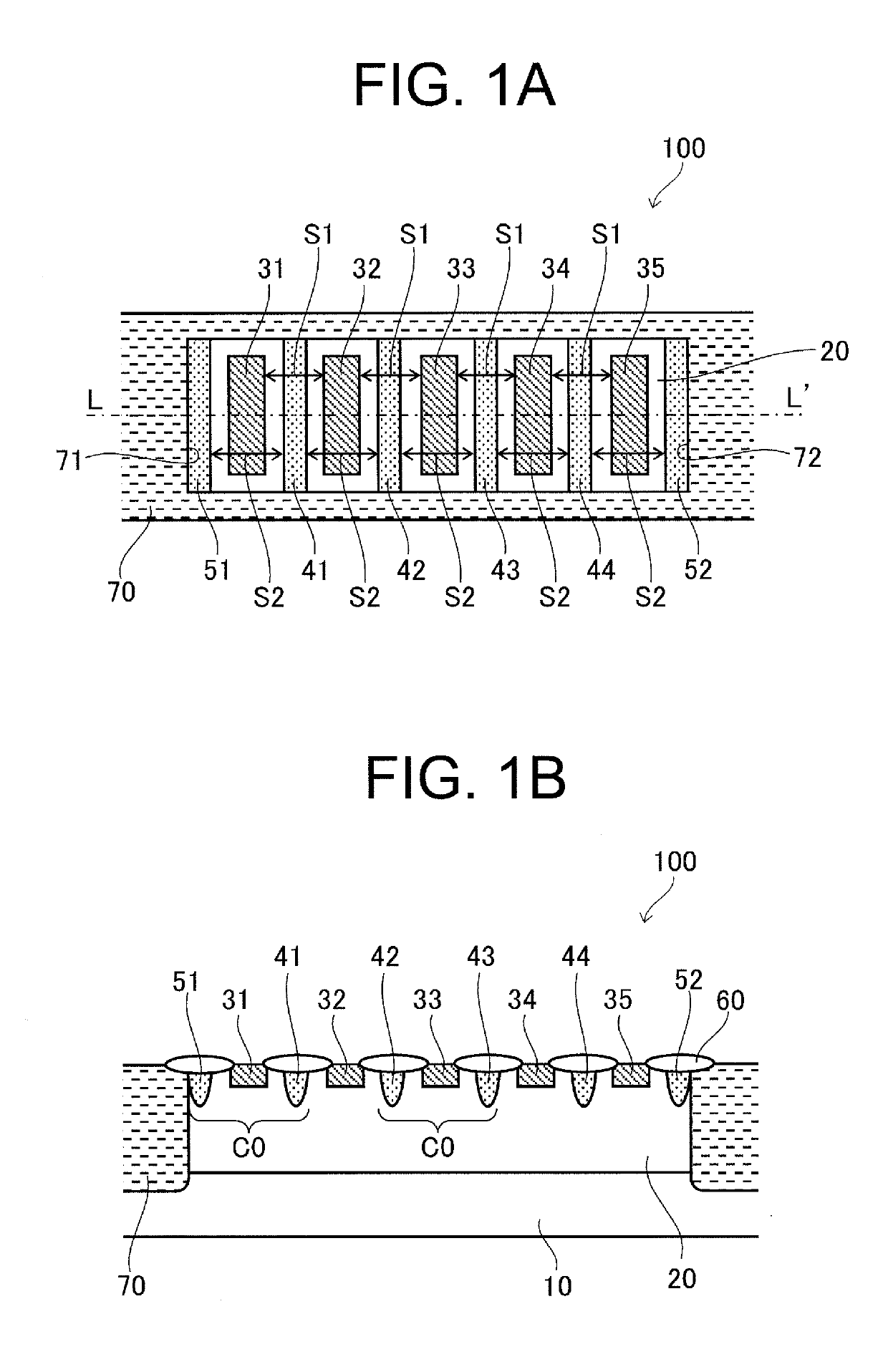
[0019]FIG. 1A and FIG. 1B are views for illustrating a semiconductor device having a vertical Hall element according to a first example of the present invention. FIG. 1A is a plan view of the semiconductor device, and FIG. 1B is a sectional view taken along the line L-L′ of FIG. 1A.

[0020]The semiconductor device of the first example of the first embodiment includes, as illustrated in FIG. 1A and FIG. 1B, a semiconductor substrate 10 of a P type which is a first conductivity type, a vertical Hall element 100 provided on the semiconductor substrate 10, and a P-type element isolation diffusion layer 70 formed so as to surround the perimeter of the vertical Hall element 100.

[0021]The vertical Hall element 100 includes a semiconductor layer 20 of an N type which is a second conductivity type, electrodes 31 to 35, electrode isolation layers 41 to 44, and added layers 51 and 52. The N-type semiconductor layer 20 is formed on the semiconductor substrate 10. The electrodes 31 to 35 are forme...

second embodiment

[0055]the present invention is described next.

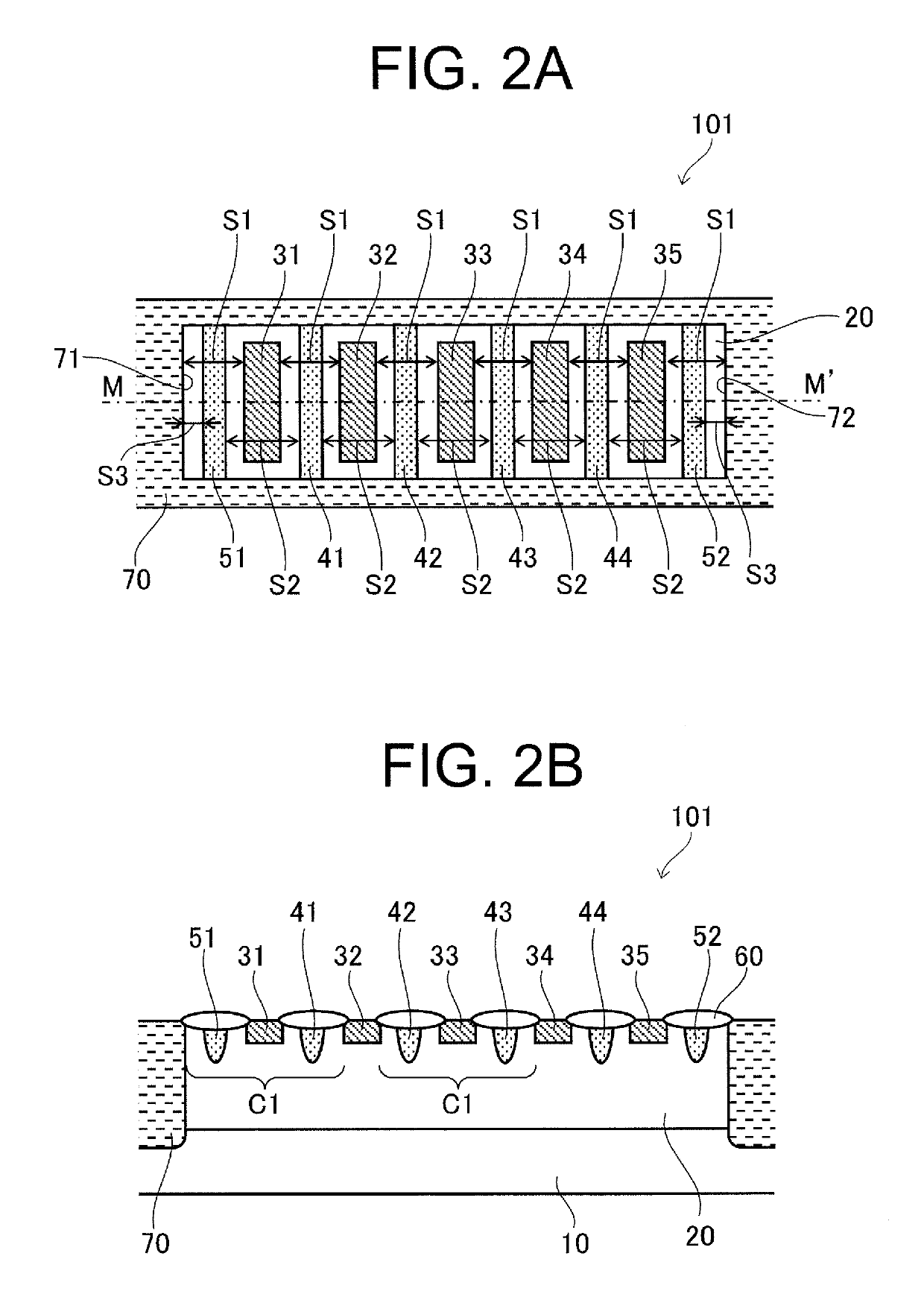
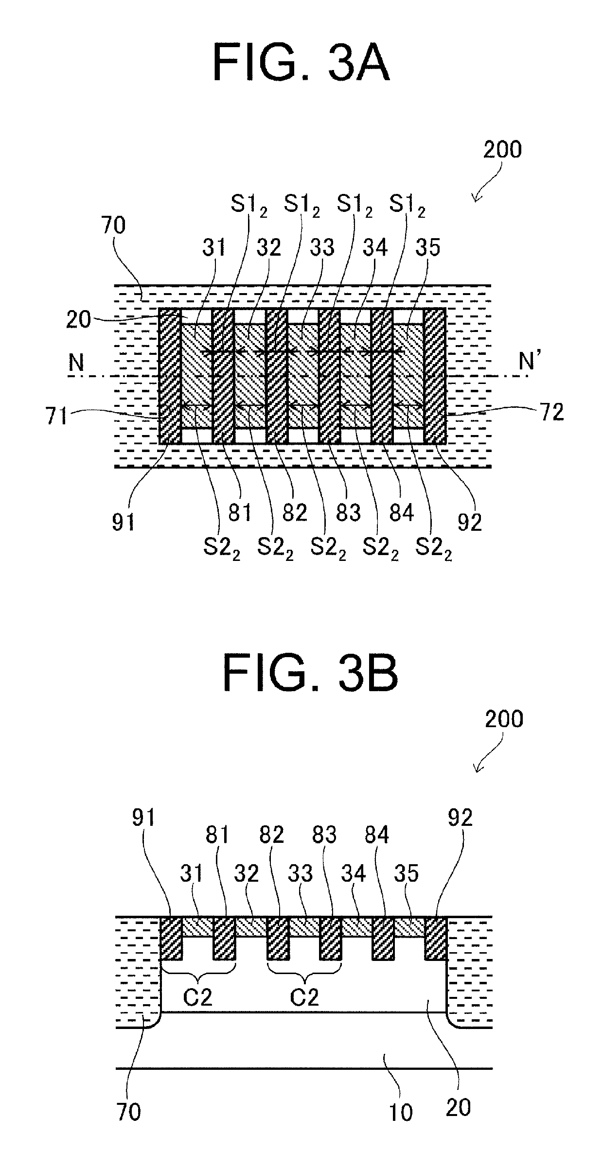
[0056]FIG. 3A is a plan view of a semiconductor device that includes a vertical Hall element according to the second embodiment of the present invention. FIG. 3B is a sectional view taken along the line N-N′ of FIG. 3A. In FIG. 3A and FIG. 3B, components that are the same as those of the semiconductor device that includes the vertical Hall element 100 illustrated in FIG. 1A and FIG. 1B are denoted by the same reference symbols, and duplicate descriptions are omitted in places.

[0057]The semiconductor device according to the second embodiment includes a vertical Hall element 200 which is provided with insulating films embedded in trenches as electrode isolation layers 81 to 84 and as added layers 91 and 92, in place of a P-type diffusion layer in the first embodiment that serves as the electrode isolation layers 41 to 44 and as the added layers 51 and 52.

[0058]Specifically, the electrodes 31 to 35 are spaced at an interval S12 along a stra...


PUM


Abstract

The vertical Hall element includes: a second conductivity type semiconductor layer formed on a first conductivity type semiconductor substrate; a plurality of high-concentration second conductivity type electrodes formed in a straight line on a surface of the semiconductor layer having substantially the same shape, and spaced at a first interval; a plurality of electrode isolation layers each formed between two electrodes out of the plurality of electrodes to isolate the plurality of electrodes from one another having substantially the same shape, and spaced at a second interval; and a first added layer and a second added layer each formed along the straight line outside of the outermost electrodes, and each having substantially the same structure as that of each electrode isolation layer.

Description

RELATED APPLICATIONS[0001]This application claims priority under 35 U.S.C. § 119 to Japanese Patent Application No. 2016-255309 filed on Dec. 28, 2016, the entire content of which is hereby incorporated by reference.BACKGROUND OF THE INVENTION1. Field of the Invention[0002]The present invention relates to a semiconductor device, in particular, to a semiconductor device having a vertical Hall element to detect a magnetic field in a horizontal direction.2. Description of the Related Art[0003]A Hall element is capable of detecting position or angle as a magnetic sensor without contacting to an object, and accordingly has various uses. Magnetic sensors that use a horizontal Hall element for detection of a magnetic field component perpendicular to a semiconductor substrate surface are particularly well known. There have been also proposed various magnetic sensors that use a vertical Hall element for detection of a magnetic field component parallel to a substrate surface.[0004]One structu...

Claims


Application Information

Patent Timeline
Patent Type & Authority Patents(United States)
IPC IPC(8): H01L43/00H01L43/06H01L43/04
CPCH01L43/04H01L43/065G01R33/07H10N52/80H10N52/101H10N50/10
Inventor HIOKA, TAKAAKIEBIHARA, MIKA
Owner ABLIC INC
Why Eureka
Try Eureka