
Per-page control of physical address space distribution among memory modules

a memory module and physical address space technology, applied in the direction of memory adressing/allocation/relocation, digital computers, instruments, etc., can solve the problems of increasing the cost of global data movement even within a processor chip, generating large amounts of global on-chip traffic within the processor, and incurring high performance and energy penalties

Active Publication Date: 2019-05-07
ADVANCED MICRO DEVICES INC
View PDF36 Cites 9 Cited by
  • Summary
  • Abstract
  • Description
  • Claims
  • Application Information

AI Technical Summary

Benefits of technology

This approach reduces global on-chip traffic and energy consumption by localizing data and computation, improving performance and energy efficiency by aligning data structures with the closest memory modules, while maintaining balanced utilization of memory channels.

Problems solved by technology

As processor chip sizes grow, global data movement even within a processor chip is becoming increasingly expensive from performance and energy perspectives.
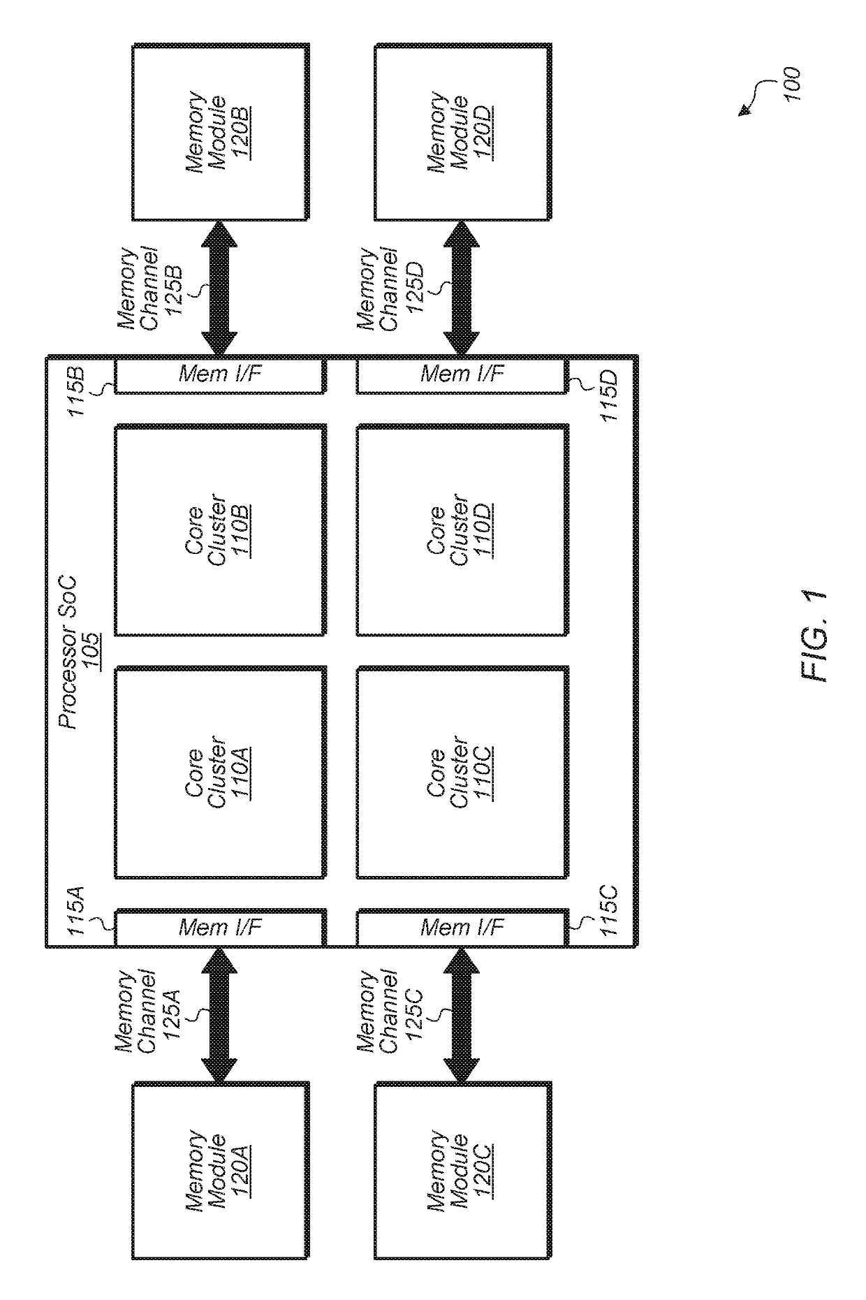
However, arbitrarily distributing computation and data across core clusters and memory modules disregards the physical proximity between core clusters and memory interfaces and generates large amounts of global on-chip traffic within the processor.
Also, performing these global memory accesses incurs high performance and energy penalties.

Method used


Image

  • Per-page control of physical address space distribution among memory modules
  • Per-page control of physical address space distribution among memory modules
  • Per-page control of physical address space distribution among memory modules

Examples


Embodiment Construction

[0015]In the following description, numerous specific details are set forth to provide a thorough understanding of the methods and mechanisms presented herein. However, one having ordinary skill in the art should recognize that the various embodiments may be practiced without these specific details. In some instances, well-known structures, components, signals, computer program instructions, and techniques have not been shown in detail to avoid obscuring the approaches described herein. It will be appreciated that for simplicity and clarity of illustration, elements shown in the figures have not necessarily been drawn to scale. For example, the dimensions of some of the elements may be exaggerated relative to other elements.

[0016]Systems, apparatuses, and methods for implementing per-page control of physical address space distribution among memory modules are disclosed herein. In one embodiment, a system includes a plurality of processing units coupled to a memory subsystem that inc...


PUM


Abstract

Systems, apparatuses, and methods for implementing per-page control of physical address space distribution among memory modules are disclosed. A computing system includes a plurality of processing units coupled to a plurality of memory modules. A determination is made as to which physical address space distribution granularity to implement for physical memory pages allocated for a first data structure. The determination can be made on a per-data-structure basis (e.g., file, page, block, etc.) or on a per-application-basis. A physical address space distribution granularity is encoded as a property of each physical memory page allocated for the first data structure, and physical memory pages of the first data structure distributed across the plurality of memory modules based on a selected physical address space distribution granularity. Page table entries (PTEs) may be annotated with the selected physical address space distribution granularity, using an addressing mapping granularity (AMG) field of a page table entry, where the granularity may be, for example, a fine-grain distribution granularity or a coarse-grain distribution granularity.

Description

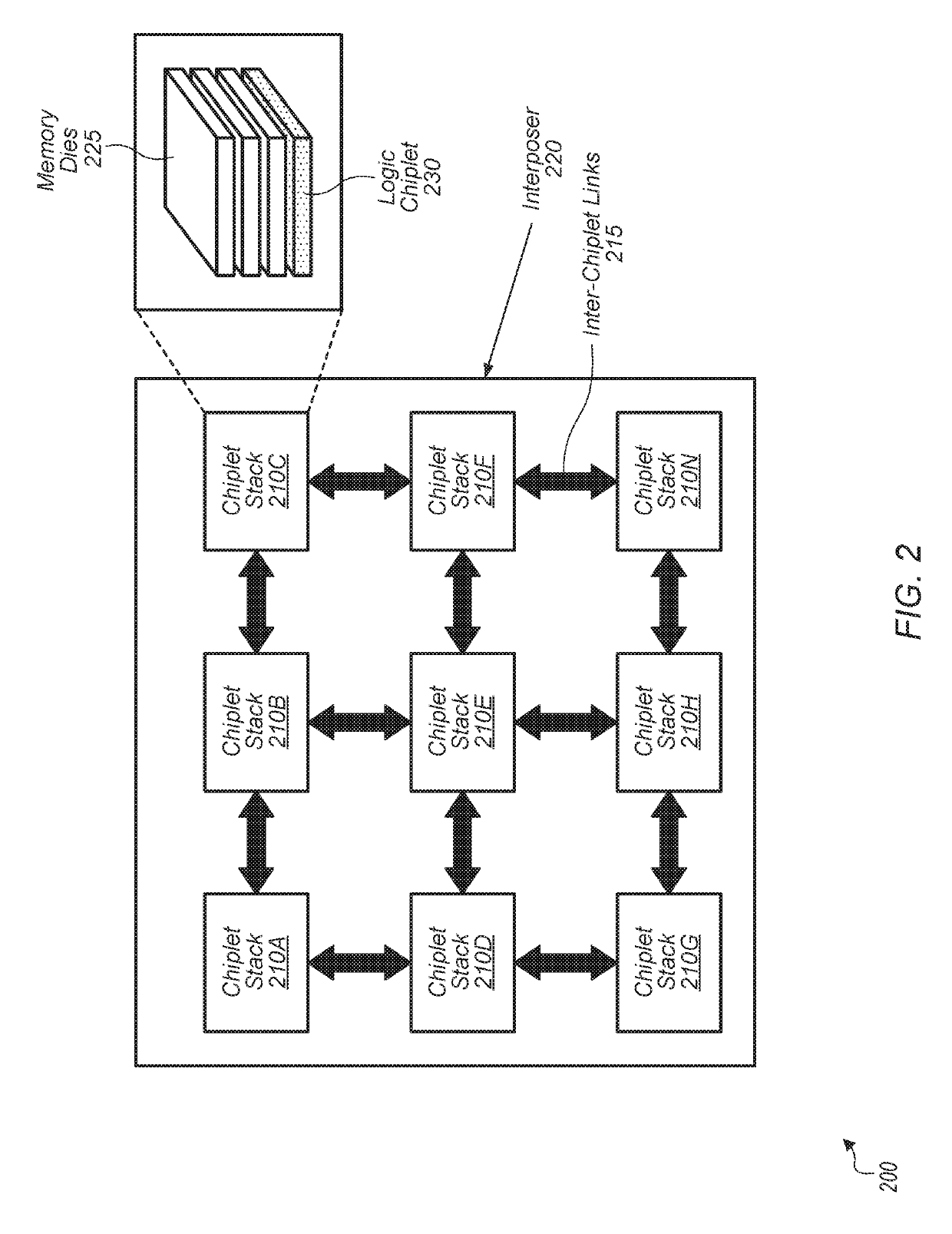
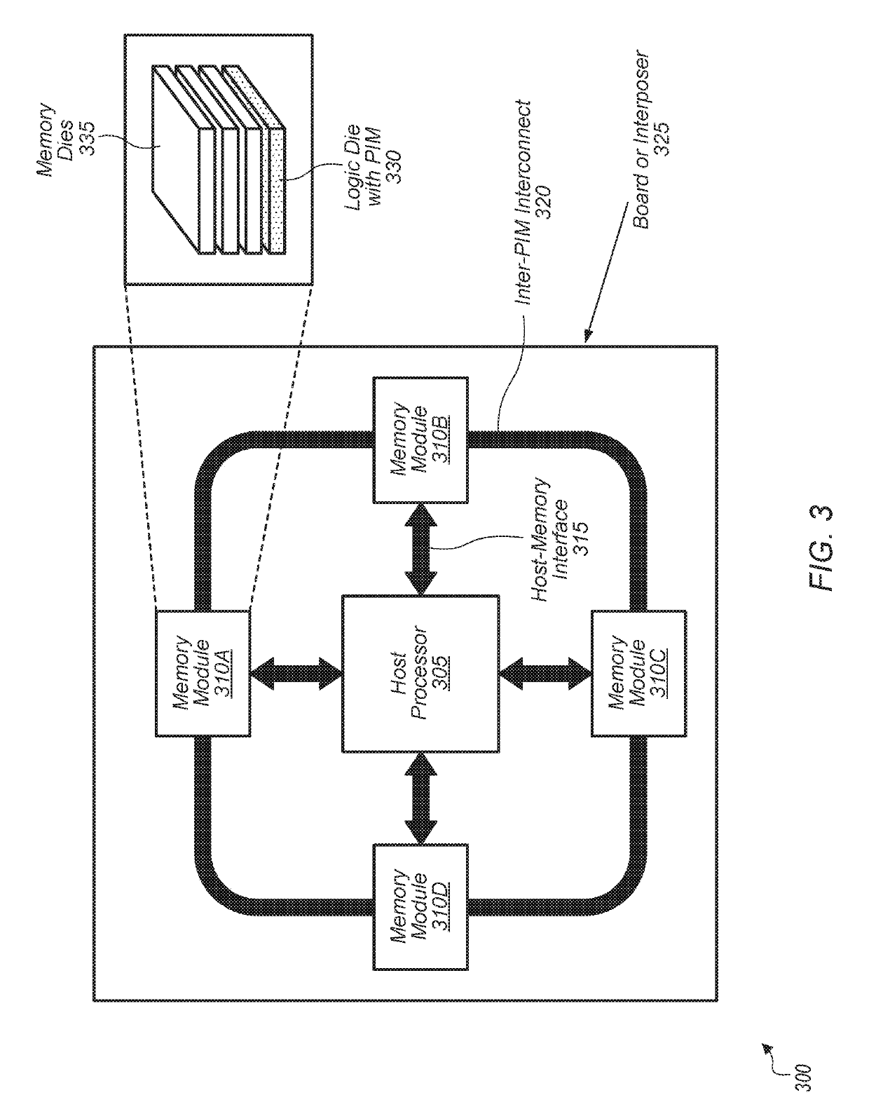
[0001]The invention described herein was made with government support under contract number DE-AC52-07NA27344, subcontract number B608045 awarded by the United States Department of Energy. The United States Government has certain rights in the invention.BACKGROUNDDescription Of The Related Art[0002]Some computing systems with a unified address space include subsets of compute units which are in close physical proximity to memory modules. For example, increasingly large systems-on chip (SoCs) and emerging silicon manufacturing and assembly technologies such as chiplet-based designs and three-dimensional (3D) die-stacking are being developed. This is leading to systems where some main memory modules have a closer association with some processing elements or cores of a processor. As processor chip sizes grow, global data movement even within a processor chip is becoming increasingly expensive from performance and energy perspectives. However, arbitrarily distributing computation and da...

Claims


Application Information

Patent Timeline
Patent Type & Authority Patents(United States)
IPC IPC(8): G06F12/10G06F12/1009G06F12/1027G06F12/06
CPCG06F12/1027G06F12/1009G06F2212/68G06F2212/656G06F12/0623G06F12/0284G06F12/0607G06F12/109G06F2212/1024G06F2212/502G06F2212/652G06F2212/657G06F15/7821
Inventor JAYASENA, NUWAN S.KIM, HYOJONGKIM, HYESOON
Owner ADVANCED MICRO DEVICES INC
Learn More