Solid-state imaging device and endoscope system
a solid-state imaging and endoscope technology, applied in the direction of optical elements, radioation control devices, instruments, etc., can solve the problems of low narrowband light image resolution and color image color resolution reduction, and achieve the effect of higher sensitivity
- Summary
- Abstract
- Description
- Claims
- Application Information
AI Technical Summary
Problems solved by technology
Method used
Image

Examples
first embodiment
(First Embodiment)
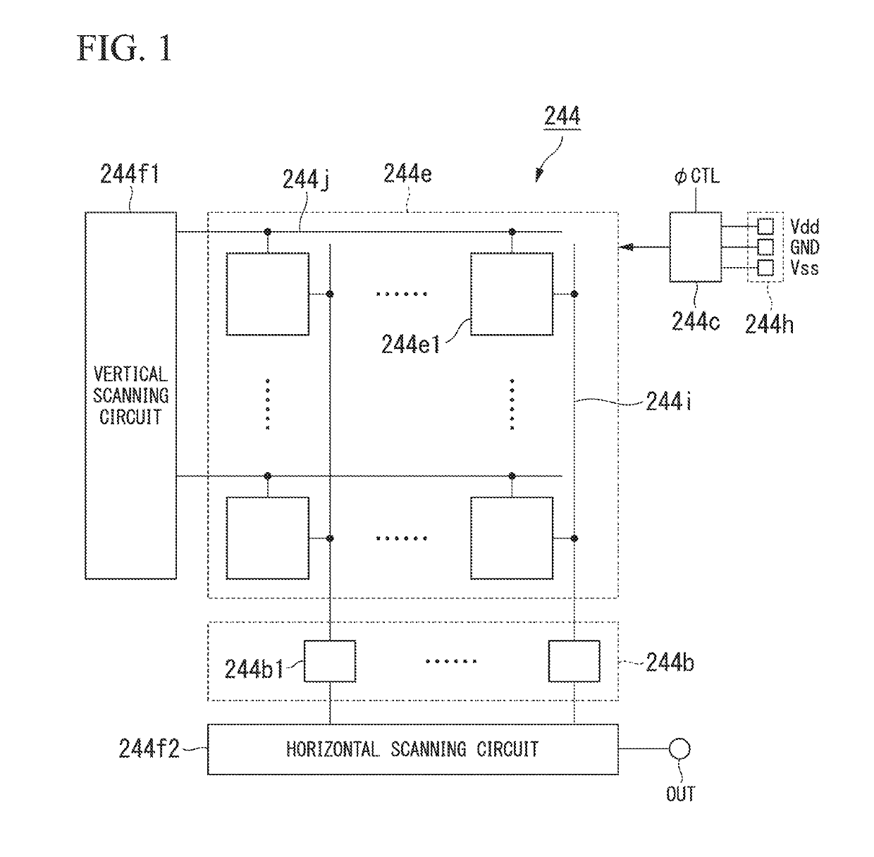
[0036]FIG. 1 shows a configuration of a solid-state imaging device 244 according to a first embodiment of the present invention. As shown in FIG. 1, the solid-state imaging device 244 includes a light receiving unit 244e (a pixel unit), an input terminal 244h, a voltage generation circuit 244c, a vertical scanning circuit 244f1, a horizontal scanning circuit 244f2, and a signal processing unit 244b. For example, the light receiving unit 244e, the input terminal 244h, the voltage generation circuit 244c, the vertical scanning circuit 244f1, the horizontal scanning circuit 244f2, and the signal processing unit 244b are arranged on the same substrate.
[0037]The light receiving unit 244e has a plurality of pixels 244e1 arranged in a matrix. In FIG. 1, a reference numeral of one pixel 244e1 is shown as a representative. Each of the plurality of pixels 244e1 generates an imaging signal corresponding to the amount of light incident on the pixel 244e1. Each of the plurality...
second embodiment
(Second Embodiment)
[0096]In a second embodiment of the present invention, the solid-state imaging device 244 of the first embodiment is replaced with a solid-state imaging device 245 shown in FIG. 8.
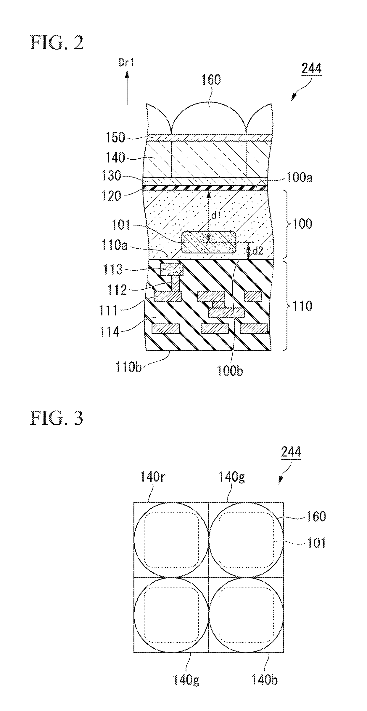
[0097]FIG. 8 shows a partial cross section of the solid-state imaging device 245. The solid-state imaging device 245 includes a semiconductor layer 100, a wiring layer 110, an insulating layer 120, contact electrodes 131, color filters 140, a resin layer 150, and microlenses 160.
[0098]Differences of the configuration shown in FIG. 8 from the configuration shown in FIG. 2 will be described. The insulating layer 120 is laminated on the semiconductor layer 100. The insulating layer 120 is in contact with the semiconductor layer 100.
[0099]The contact electrodes 131 are buried in the insulating layer 120. Each of the contact electrodes 131 is made of a material having conductivity. For example, the contact electrode 131 is a metal such as tungsten (W). The contact electrodes 131 are disposed ...
third embodiment
(Third Embodiment)
[0107]In a third embodiment of the present invention, the solid-state imaging device 244 of the first embodiment is replaced with a solid-state imaging device 246 shown in FIG. 10.
[0108]FIG. 10 shows a partial cross section of the solid-state imaging device 246. The solid-state imaging device 246 includes a semiconductor layer 102, a wiring layer 110, an insulating layer 120, transparent electrodes 132, color filters 140, a resin layer 150, and microlenses 160.
[0109]Differences of the configuration shown in FIG. 10 from the configuration shown in FIG. 2 will be described. In FIG. 10, the semiconductor layer 100 in FIG. 2 is replaced with a semiconductor layer 102. The semiconductor layer 102 has a surface 102a (a first surface) and a surface 102b (a second surface). The surface 102a of the semiconductor layer 102 is the back surface of the semiconductor layer 102. The surface 102a of the semiconductor layer 102 is in contact with the insulating layer 120. The surfa...
PUM
 Abstract
Description
Claims
Application Information