

Compound thin-film solar cell and process for producing the same
a solar cell and semiconductor technology, applied in the field of compound semiconductor thin-film solar cells, can solve the problems of easy deformation, small band gap of ins buffer layer, and general difficulty in passing light of short wavelengths, etc., to achieve the effect of increasing the size of particles to be deposited, improving grain structure, and increasing the temperature of aqueous solution
- Summary
- Abstract
- Description
- Claims
- Application Information
AI Technical Summary
Benefits of technology
Problems solved by technology
Method used
Image

Examples
Embodiment Construction
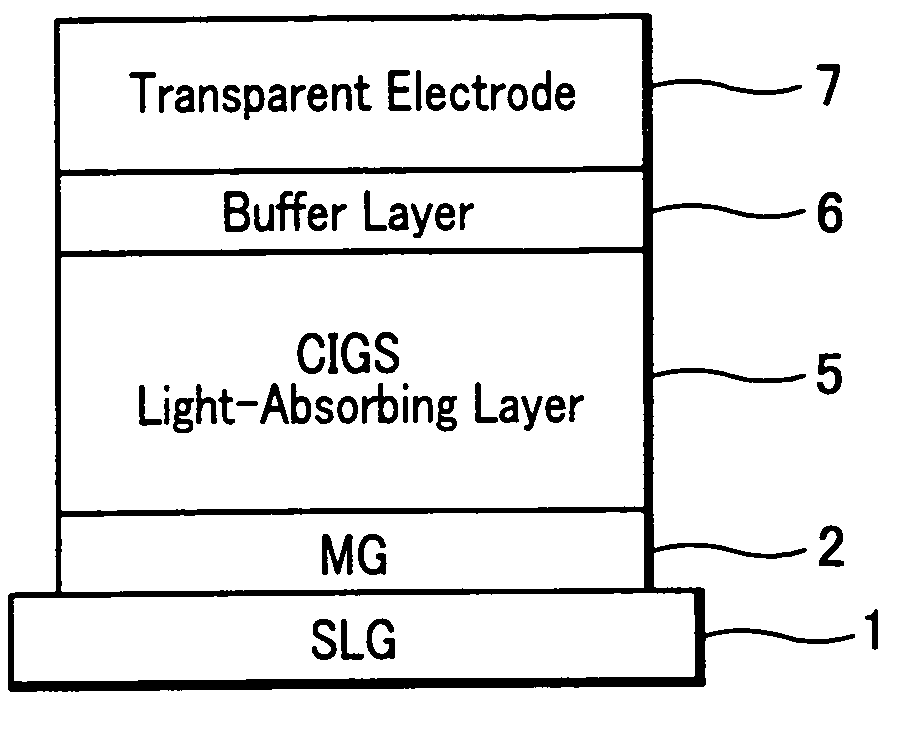
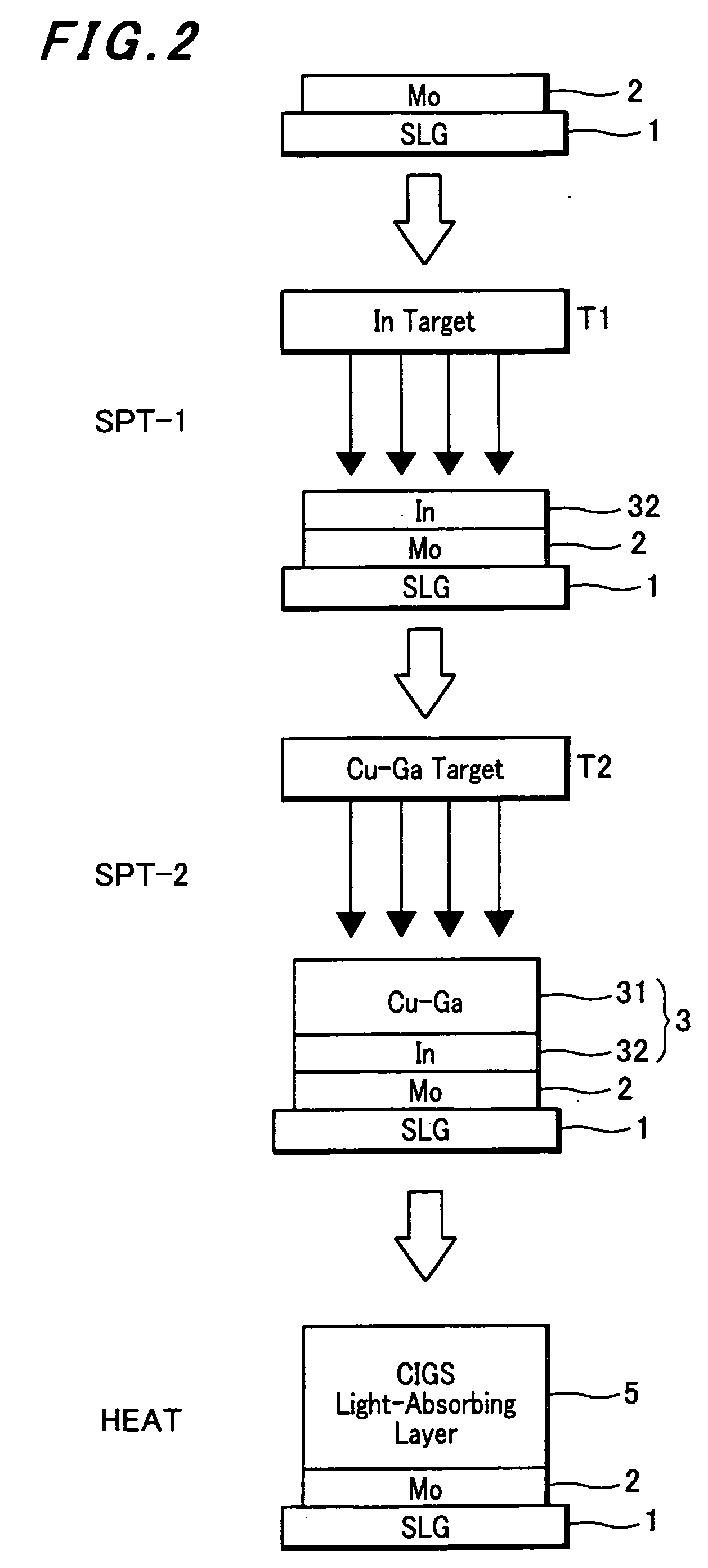
[0017] In FIGS. 2 and 3, there is shown a process of fabricating a compound semiconductor thin-film solar cell.
[0018] As shown in FIG. 2, a molybdenum (Mo) electrode layer 2 serving as a back electrode is first formed by sputtering on a SLG (soda lime glass) substrate 1. Next, an indium (In) layer 32 is formed on the back electrode layer 2 by the first sputtering process SPT-1 using a single In target T1 and a copper-gallium (Cu—Ga) alloy layer 31 is formed thereon by the second sputtering process SPT-2 using a Cu—Ga alloy target T2 to form a laminated metal precursor 3 composed of the In layer 32 and the Cu—Ga alloy layer 31. The precursor 3 is then treated by heat (by the heat treatment process HEAT) in the atmosphere of selenium (Se) to form a thin film light absorbing layer 5 of CIGS.
[0019] As described above, a laminated precursor 3 is fabricated by forming first an In layer 32 and then a Cu—Ga alloy layer 31 on a Mo electrode layer 2, thereby preventing the formation of an a...
PUM
 Abstract
Description
Claims
Application Information