
Array substrate, color filter substrate, and manufacturing methods thereof, display panel and display device

a technology of color filter substrate and array substrate, which is applied in the field of array substrate, color filter substrate, and manufacturing methods thereof, can solve the problems of low switchover efficiency and increase the cost of the prior art transparent display device, and achieve the effect of simple operation and high switchover efficiency

Active Publication Date: 2019-06-25
BOE TECH GRP CO LTD +1
View PDF16 Cites 1 Cited by
  • Summary
  • Abstract
  • Description
  • Claims
  • Application Information

AI Technical Summary

Benefits of technology

This approach allows for cost-effective and efficient switching between transparent and non-transparent displays by modifying the scanning sequence of gate lines, eliminating the need for additional components and simplifying the switching process.

Problems solved by technology

In the prior art, to realize the switchover between the transparent display and the non-transparent display, a light blocking part (such as the blocking device or the color changing layer) is required to be additionally set in the transparent display device, so that the cost of the transparent display device in the prior art is increased.
Meanwhile, the operation to switch between the transparent display and the non-transparent display in the prior art is complicated, resulting in a low switchover efficiency.

Method used


Image

  • Array substrate, color filter substrate, and manufacturing methods thereof, display panel and display device
  • Array substrate, color filter substrate, and manufacturing methods thereof, display panel and display device
  • Array substrate, color filter substrate, and manufacturing methods thereof, display panel and display device

Examples


embodiment 1

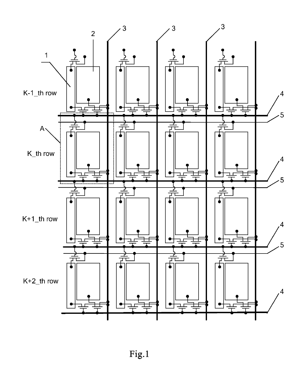
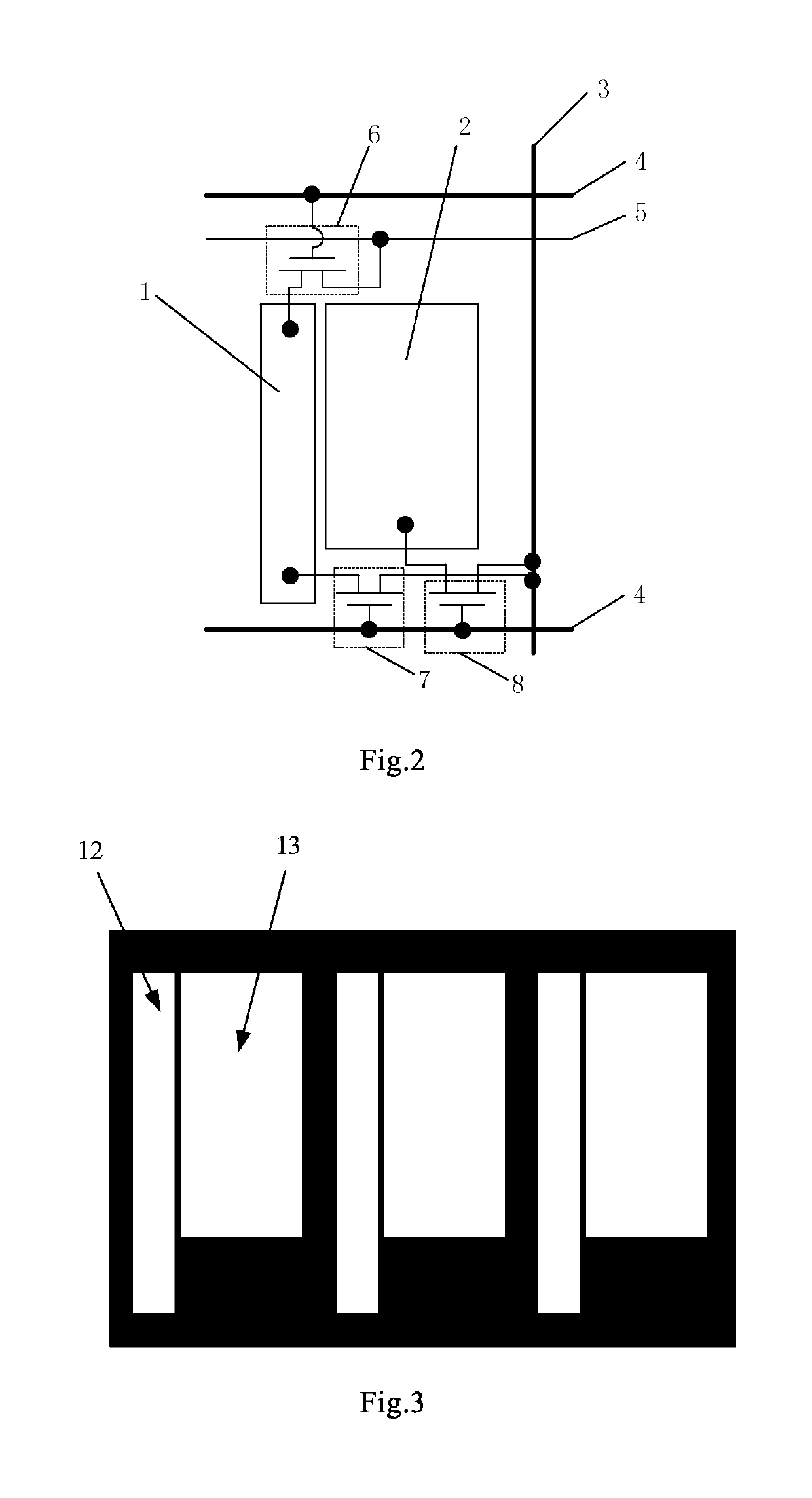
[0059]FIG. 1 is a schematic diagram of a structure of an array substrate provided by Embodiment 1 of the present invention, and FIG. 2 is a partially enlarged view of a structure A in FIG. 1. As shown in FIG. 1 and FIG. 2, the array substrate includes a plurality of gate lines 4 and a plurality of data lines 3, wherein the gate lines 4 and the data lines 3 define pixel units, and the pixel units each is provided therein with a second electrode 2 and switch units. A part or all of the pixel units each are provided therein with a first electrode 1, and the switch units are used for controlling the first electrode 1 and the second electrode 2 to be loaded with voltage signals. When the gate lines 4 are sequentially scanned, the first electrode 1 is loaded with a first voltage signal, and when the gate lines 4 are reversely scanned, the first electrode 1 is loaded with a second voltage signal; and when the gate lines 4 are sequentially scanned, the second electrode 2 is loaded with a th...

embodiment 2

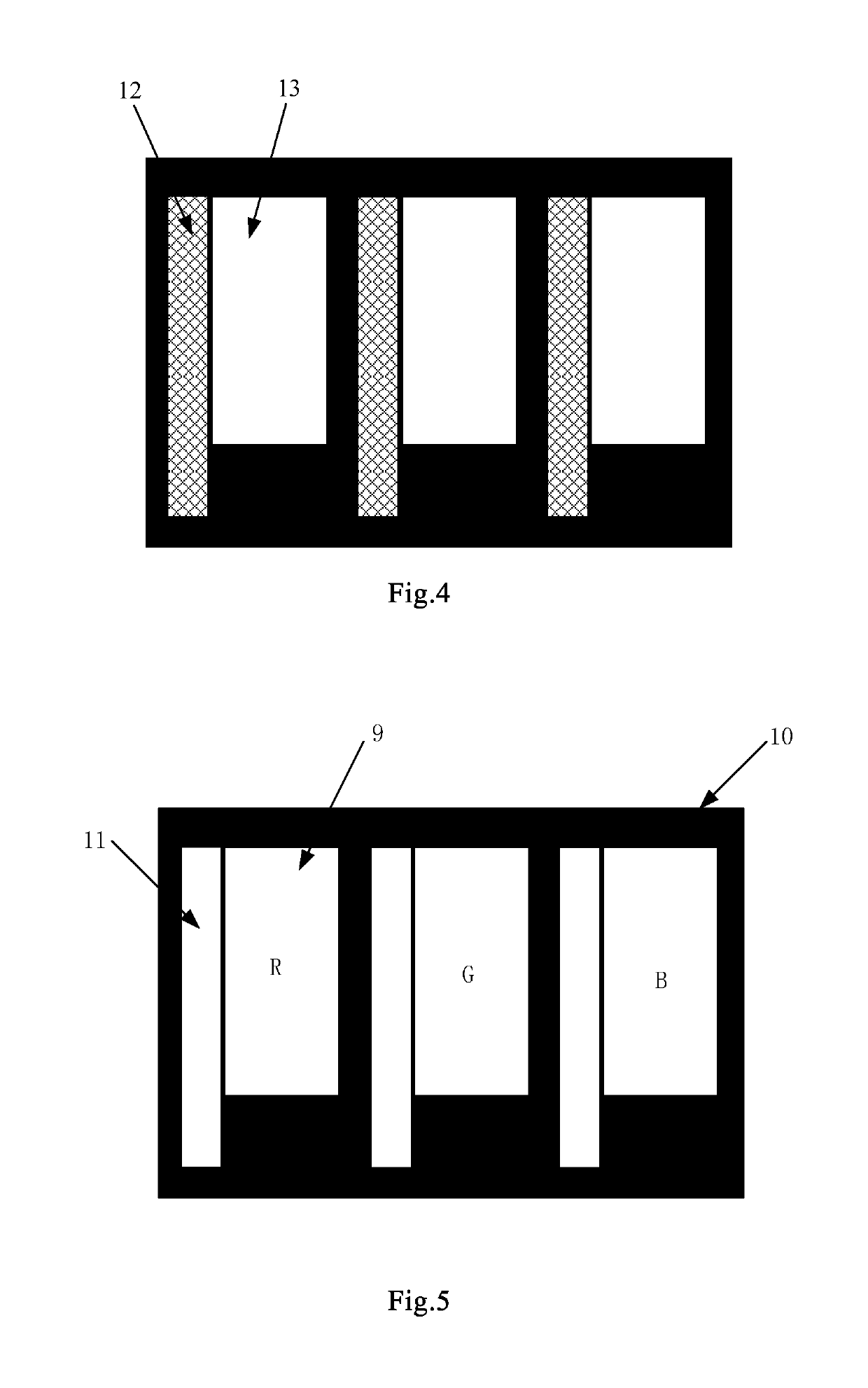
[0090]FIG. 5 is a schematic diagram of a partial structure of a color filter substrate provided by Embodiment 2 of the present invention. As shown in FIG. 5, the color filter substrate includes light blocking strips 10 provided on a second base substrate, by which a plurality of pixel regions are defined. The pixel region is formed therein with a color matrix pattern 9, and at least part of the pixel regions each is formed therein with a transparent pattern 11. In the example shown in FIG. 5, three adjacent light blocking strips 10 are shown, and the three light blocking strips 10 define three pixel units.

[0091]In this case, the color matrix pattern 9 may include a red matrix pattern R, a green matrix pattern G and a blue matrix pattern B, and of course, the color matrix pattern 9 may also be a matrix pattern of any other color. Meanwhile, the light blocking strip may be a black matrix or any other unit formed with a light blocking material.

[0092]In this embodiment, in a display dev...

embodiment 3

[0097]Embodiment 3 of the present invention provides a display panel, including an array substrate and a color filter substrate provided opposite to each other, wherein the array substrate provided by Embodiment 1 is adopted as the array substrate, the color filter substrate provided by Embodiment 2 is adopted as the color filter substrate, the pixel unit is provided in correspondence with the pixel region, the first electrode is provided in correspondence with the transparent pattern and the second electrode is provided in correspondence with the color matrix pattern. The details thereof may refer to the descriptions of Embodiments 1 and 2, and will not be redundantly described herein.

[0098]It is noted that, the display panel in Embodiment 3 includes any one of a Twisted Nematic (TN) panel, a Vertical Alignment (VA) panel, an In-Plane Switching (IPS) panel and a Fringe Field Switching (FFS) panel.

[0099]Embodiment 3 of the present invention provides a display panel, including an arr...


PUM

PropertyMeasurementUnit
transparentaaaaaaaaaa
voltageaaaaaaaaaa
non-transparentaaaaaaaaaa

Abstract

The invention discloses an array substrate, a color substrate, and manufacturing methods thereof, a display panel and a display device. The array substrate includes a plurality of gate lines and a plurality of data lines provided on a first base substrate to be intersected with each other, the gate lines and the data lines define a plurality of pixel units and at least part of the pixel units each provided therein with a first electrode, when the plurality of gate lines are sequentially scanned, the first electrode is loaded with a first voltage signal and a region corresponding to the first electrode is in a transparent state, and when the plurality of gate lines are reversely scanned, the first electrode is loaded with a second voltage signal, and a region corresponding to the first electrode is in a non-transparent state. The invention realizes a high switchover efficiency.

Description

[0001]This is a National Phase Application filed under 35 U.S.C. 371 as a national stage of PCT / CN2014 / 076950, filed May 7, 2014, an application claiming the benefit of Chinese Application No. 201310626530.2, filed Nov. 28, 2013, the content of each of which is hereby incorporated by reference in its entirety.FIELD OF THE INVENTION[0002]The present invention relates to the field of display technology, and particularly relates to an array substrate, a color filter substrate, and manufacturing methods thereof, a display panel and a display device.BACKGROUND OF THE INVENTION[0003]Recently, as the development of display technology, manufacturers successively release a series of transparent display devices, display modes of which include a transparent display mode and a non-transparent display mode. Here, the so-called transparent display refers to the mode in which an object behind a display device can be seen through the display device when a user is using the display device; and the s...

Claims


Application Information

Patent Timeline
Patent Type & Authority Patents(United States)
IPC IPC(8): G02B5/20G09G3/38H01L27/12G02F1/1343G02F1/1362G09G3/36
CPCH01L27/124G02F1/13624G02F1/134309G02F1/136286G09G3/3607G09G3/3648G09G3/38H01L27/127G02B5/201G09G2310/0283G09G2300/0426G09G2300/0456G09G2300/0814G09G2310/0251G09G2310/0262
Inventor CHEN, HUABINYUAN, JIANFENG
Owner BOE TECH GRP CO LTD
Learn More