Back-channel-etched TFT substrate and manufacturing method thereof

a technology of backchannel etching and thin film transistor, which is applied in the direction of semiconductor devices, electrical devices, transistors, etc., can solve the problems of affecting the performance of the tft device, affecting the manufacturing process of igzo tft with esl structure, and reducing the cost of disabling cost reduction, so as to reduce the probability of forming unbalance, reduce the probability of forming, and reduce the deposition power

Inactive Publication Date: 2019-06-25
SHENZHEN CHINA STAR OPTOELECTRONICS SEMICON DISPLAY TECH CO LTD
View PDF7 Cites 0 Cited by
  • Summary
  • Abstract
  • Description
  • Claims
  • Application Information

AI Technical Summary

Benefits of technology

[0013]The object of the present invention is to provide a manufacturing method of the back-channel-etched (BCE) TFT substrate, able to ensure that the side of the passivation layer in contact with the air is more hydrophobic and prevents the outside water from entering the back-channel while ensuring that the side of the passivation layer in contact with the IGOZ active layer has a lower oxygen content and reduces the probability of forming unbalanced O-ion at the interface of the passivation layer and the IGZO active layer, at the same time to prevent the source and drain from oxidization, to ensure stable device performance.
[0014]Another object of the present invention is to provide a BCE TFT substrate, with stronger device stability.
[0019]According to a preferred embodiment of the present invention, when depositing the first silicon oxide thin film and the second silicon oxide thin film by the plasma enhanced chemical vapor deposition process, the deposition power of the second silicon oxide thin film is greater than the deposition power of the first silicon oxide thin film so that bond angle of Si—O—Si bond in the second silicon oxide thin film is smaller than bond angle of Si—O—Si bond in the first silicon oxide thin film and the second silicon oxide thin film is more hydrophobic the first silicon oxide thin film.
[0037]The present invention provides the following advantages. The manufacturing method of BCE TFT substrate of the present invention uses low deposition power and low oxygen content to deposit a first silicon oxide thin film and then increases the deposition power and maintains a low oxygen content to deposit a second silicon oxide thin film on the first silicon oxide thin film. The first and second silicon oxide thin films form a passivation layer, and finally, the second silicon oxide film is implanted with oxygen by an ion implantation process to form a superficial layer so that the Si:O atomic ratio in the superficial layer is close to or same as Si:O atomic ratio of SiO2, to ensure that the passivation layer in contact with the air side is strongly hydrophobic to prevent outside water vapor into the back-channel, while ensuring that the side of passivation layer contacting IGZO active layer has a lower oxygen content to reduce the probability of forming unbalanced O-ions at the interface between the passivation layer and the IGZO active layer, and at the same time prevents the source and drain from being oxidized to ensure stable device performance. The BCE TFT substrate of the invention is prepared by the above method, and has strong device stability.

Problems solved by technology

However, the manufacturing process of IGZO TFT with ESL structure is complicated and requires six photolithography processes, which is disabling for cost reduction.
When any one balance is destroyed, the performance of the TFT device will be affected.

Method used


Image

  • Back-channel-etched TFT substrate and manufacturing method thereof
  • Back-channel-etched TFT substrate and manufacturing method thereof
  • Back-channel-etched TFT substrate and manufacturing method thereof

Examples


Embodiment Construction

[0043]To further explain the technique means and effect of the present invention, the following uses preferred embodiments and drawings for detailed description.

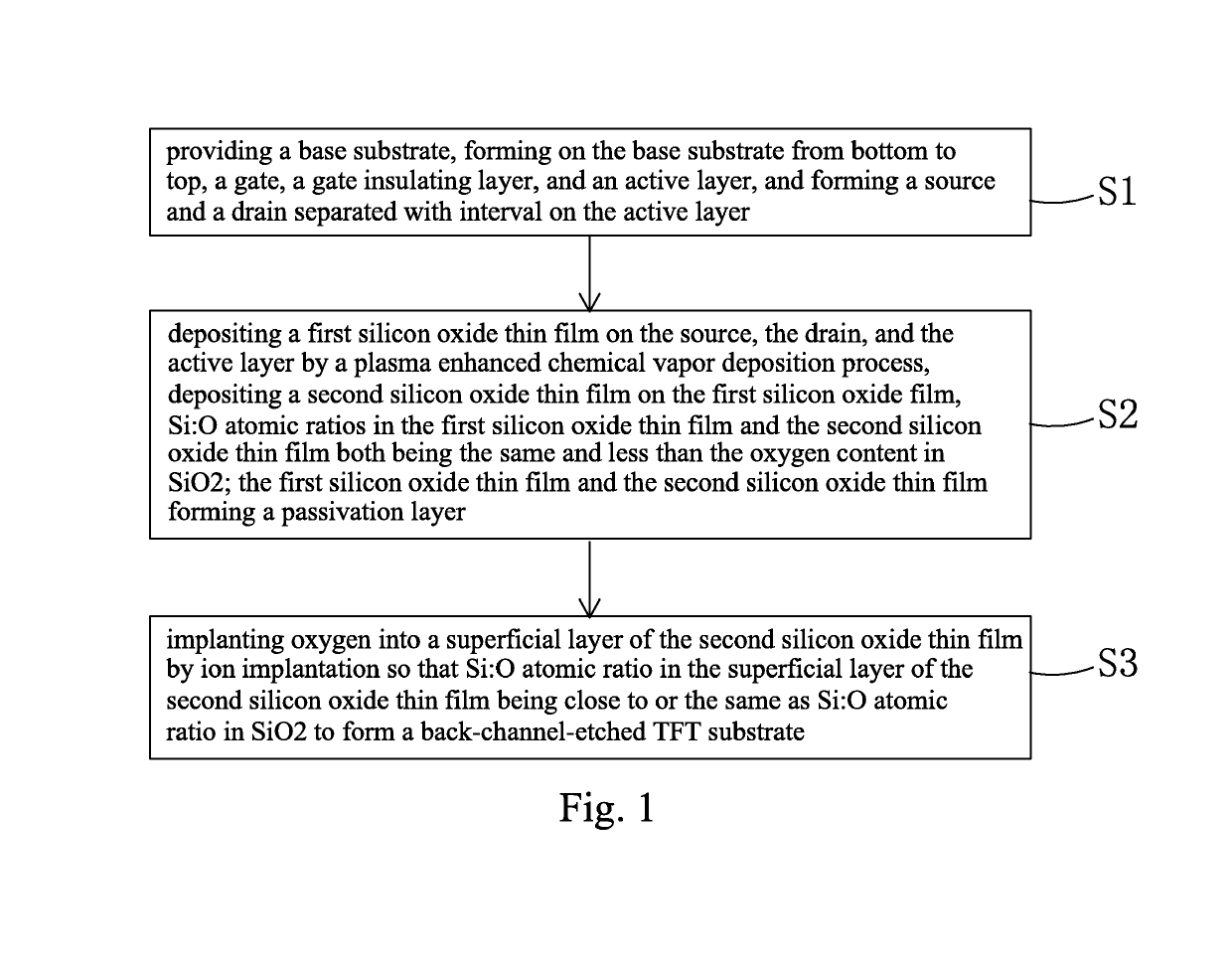
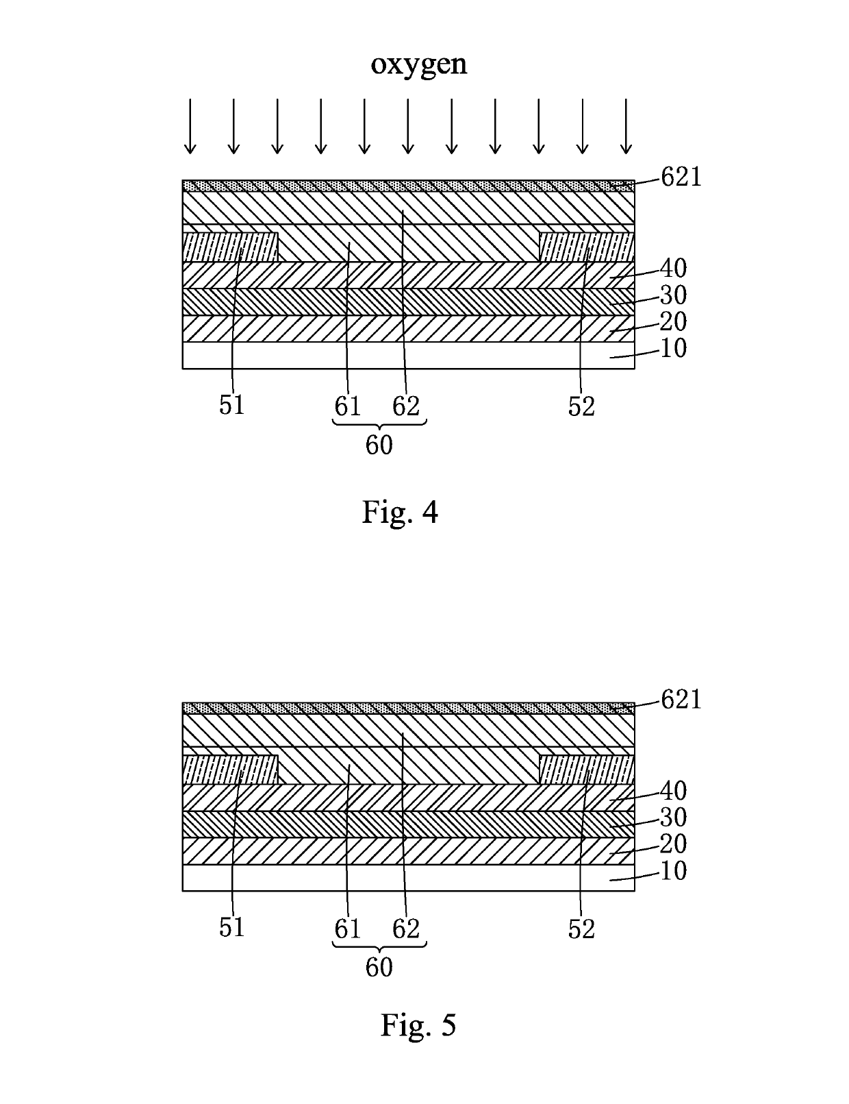
[0044]Referring to FIG. 1, the present invention provides a manufacturing method of back-channel-etched TFT substrate, comprising:

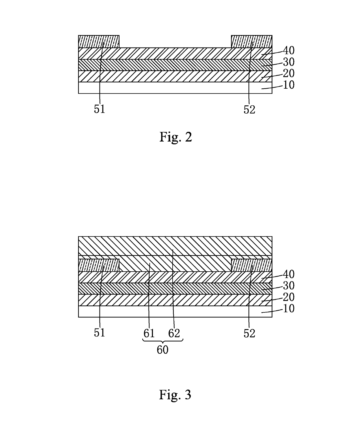
[0045]Step S1: as shown in FIG. 2, providing a base substrate 10, forming on the base substrate 10 from bottom to top, a gate 20, a gate insulating layer 30, and an active layer 40, and forming a source 51 and a drain 52 separated with interval on the active layer 40.

[0046]Specifically, the material of the gate insulating layer 30 comprises SiOx; the material of the active layer 40 comprises IGZO; and the material of the source 51 and the drain 52 comprises Cu.

[0047]Step S2: as shown in FIG. 3, depositing a first silicon oxide thin film 61 on the source 51, the drain 52, and the active layer 40 by a plasma enhanced chemical vapor deposition (PECVD) process, depositing a second silicon oxide thin f...


PUM

PropertyMeasurementUnit
leakage currentaaaaaaaaaa
driving frequencyaaaaaaaaaa

Abstract

The invention provides a BCE TFT substrate and manufacturing method thereof. The method uses low deposition power and low oxygen content to deposit first silicon oxide thin film; then increases deposition power with low oxygen content to deposit second silicon oxide thin film. The first and second silicon oxide thin films form a passivation layer; the second silicon oxide film is implanted with oxygen to form a superficial layer so that the Si:O atomic ratio in the superficial layer is close to or same as Si:O atomic ratio of SiO2, to ensure the passivation layer in contact with the air side is strongly hydrophobic to prevent outside water vapor into the back-channel, while ensuring the side of passivation layer contacting IGZO active layer has a lower oxygen content to reduce the probability of forming unbalanced O-ions at the interface between passivation layer and IGZO active layer.

Description

BACKGROUND OF THE INVENTION1. Field of the Invention[0001]The present invention relates to the field of display techniques, and in particular to a back-channel-etched thin film transistor (TFT) substrate and manufacturing method thereof.2. The Related Arts[0002]The liquid crystal display (LCD) provides advantages of thinness, low power-consumption and no radiation, and is widely used in, such as, LCD televisions, mobile phones, personal digital assistants (PDAs), digital cameras, computer screens, laptop screens, and so on.[0003]The organic light-emitting diode (OLED) display device, also called organic electroluminescent display, is a new type of panel display device. Because the OLED display device provides the advantages of simple manufacturing process, low cost, low power consumption, high luminous efficiency, wide temperature range operation, thinness and lightness, short response time, ability to achieve color display and large-screen display, easy to realize matching with IC ...

Claims


Application Information

Patent Timeline
Patent Type & Authority Patents(United States)
IPC IPC(8): H01L27/12H01L29/786H01L29/49H01L29/45H01L29/66H01L29/417H01L21/3213H01L29/423
CPCH01L29/66969H01L21/3213H01L27/1203H01L27/1214H01L27/1251H01L29/786H01L29/41733H01L29/42384H01L29/45H01L29/4908H01L29/66742H01L27/1262H01L27/1259H01L21/02164H01L21/02274H01L21/02323H01L21/31155H01L29/7869H01L27/1248H01L29/78696H01L29/458
Inventor JIANG, CHUNSHENG
Owner SHENZHEN CHINA STAR OPTOELECTRONICS SEMICON DISPLAY TECH CO LTD
Why Eureka
Try Eureka