Digital-to-analog converter (DAC) circuits employing resistor rotator circuits configured to be included in analog-to-digital converter (ADC) circuits

Active Publication Date: 2019-06-25
QUALCOMM INC
View PDF22 Cites 2 Cited by
  • Summary
  • Abstract
  • Description
  • Claims
  • Application Information

AI Technical Summary

Benefits of technology

[0005]Aspects disclosed in the detailed description include digital-to-analog converter (DAC) circuits employing resistor rotator circuits configured to be included in analog-to-digital converter (ADC) circuits. In one aspect, a DAC circuit includes multiple DAC stages, each of which may be configured to generate one or more DAC analog signals corresponding to a selected resistance of the DAC stage. In particular, each DAC stage is configured to receive a corresponding top voltage and a corresponding bottom voltage. Each DAC stage is configured to generate a number of DAC analog signals based on the corresponding top voltage and the corresponding bottom voltage. Additionally, one or more DAC stages include an adjusting circuit comprising a resistance configured to adjust a resistance of the corresponding DAC stage such that a parallel combination of the resistance of the adjusting circuit and a resistance of a next DAC stage is maintained at an ideal resistance level. Employing multiple DAC stages and the adjusting circuits in this manner results in the DAC circuit employing less circuitry, and thus, consuming less area, than conventional DAC circuits.
[0006]In this regard in one aspect, a multiple-bit parallel SAR ADC circuit is provided, and comprises a plurality of SAR controller circuits. Each SAR controller circuit of the plurality of SAR controller circuits comprises a number of SAR register circuits. Each SAR register circuit is configured to receive a clock signal, and, in response to a corresponding cycle of the clock signal, provide a digital signal for a digital bit of the digital output signal. Each SAR register circuit is further configured to, in response to a corresponding next cycle of the clock signal, receive a corresponding digital bit, store the digital bit, and provide the digital signal correlating to the digital bit. The digital bit is based on a comparison of an analog input signal and a corresponding DAC analog signal. The multiple-bit parallel SAR ADC circuit further comprises a multiple-output DAC circuit comprising a plurality of DAC stages. Each DAC stage of the plurality of DAC stages is configured to receive a corresponding top voltage and a corresponding bottom voltage, wherein a voltage range of the corresponding top voltage and the corresponding bottom voltage is based on a reference voltage, and generate a number of DAC analog signals based on the corresponding top voltage, the corresponding bottom voltage, and a resistance of the DAC stage. Each DAC stage of the plurality of DAC stages comprises an adjusting circuit comprising a resistance configured to adjust the resistance of the corresponding DAC stage such that a parallel combination of the resistance of the adjusting circuit and a resistance of a next DAC stage is maintained at an ideal resistance level. The multiple-bit parallel SAR ADC circuit further comprises a compare circuit. The compare circuit is configured to receive the number of DAC analog signals, receive the analog input signal, and generate the digital bit corresponding to each SAR controller circuit of the plurality of SAR controller circuits based on a comparison of each DAC analog signal to the analog input signal. Each digital bit generated collectively forms a digital output signal that is a digital representation of the analog input signal.
[0007]In another aspect, a method for converting an analog input signal into a digital output signal is provided, wherein multiple digital bits of the digital output signal are generated in parallel. The method comprises receiving a reference voltage, receiving a clock signal, and, in response to a corresponding cycle of the clock signal, providing a digital signal. The method also comprises, in response to a corresponding next cycle of the clock signal, receiving a corresponding digital bit, wherein the digital bit is based on a comparison of the analog input signal and a corresponding DAC analog signal. The method further comprises, in response to the corresponding next cycle of the clock signal, storing the digital bit, and, in response to the corresponding next cycle of the clock signal, providing the digital signal correlating to the digital bit. The method also comprises receiving a corresponding top voltage and a corresponding bottom voltage, wherein a voltage range of the corresponding top voltage and the corresponding bottom voltage is based on the reference voltage. The method further comprises generating a number of DAC analog signals based on the corresponding top voltage, the corresponding bottom voltage, and a resistance of a DAC stage, wherein the number of DAC analog signals is equal to a number of

Problems solved by technology

Employing multiple DAC stages and the adjusting circuits in this manner results in the DAC ci

Method used


Image

  • Digital-to-analog converter (DAC) circuits employing resistor rotator circuits configured to be included in analog-to-digital converter (ADC) circuits
  • Digital-to-analog converter (DAC) circuits employing resistor rotator circuits configured to be included in analog-to-digital converter (ADC) circuits
  • Digital-to-analog converter (DAC) circuits employing resistor rotator circuits configured to be included in analog-to-digital converter (ADC) circuits

Examples


Embodiment Construction

[0041]With reference now to the drawing figures, several exemplary aspects of the present disclosure are described. The word “exemplary” is used herein to mean “serving as an example, instance, or illustration.” Any aspect described herein as “exemplary” is not necessarily to be construed as preferred or advantageous over other aspects.

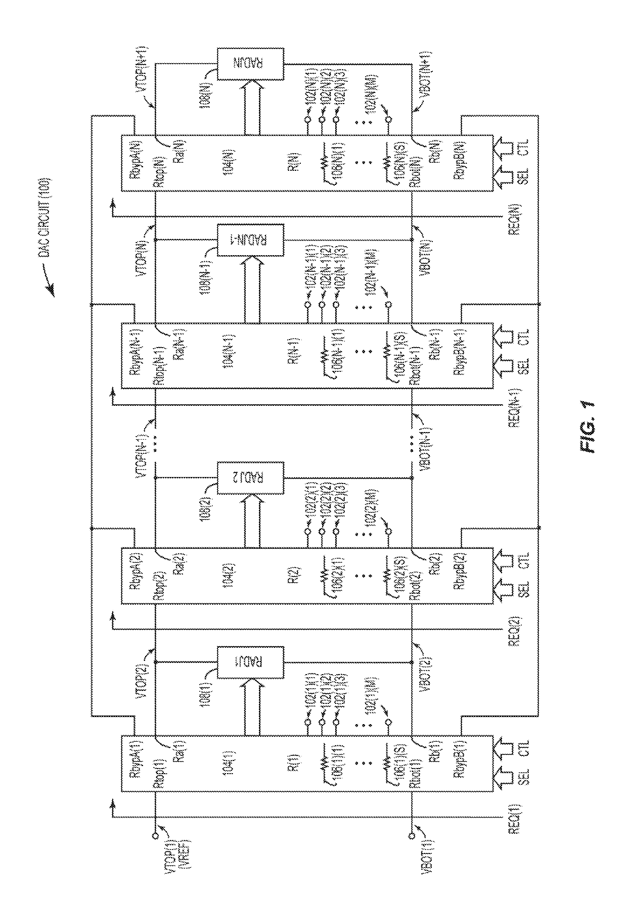
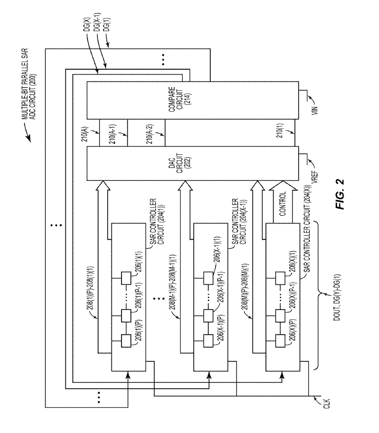
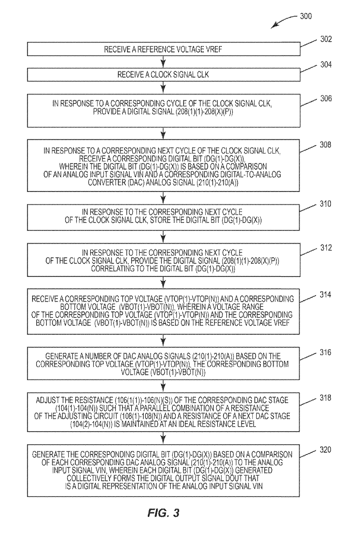
[0042]Aspects disclosed in the detailed description include digital-to-analog converter (DAC) circuits employing resistor rotator circuits configured to be included in analog-to-digital converter (ADC) circuits. In one aspect, a DAC circuit includes multiple DAC stages, each of which may be configured to generate one or more DAC analog signals corresponding to a selected resistance of the DAC stage. In particular, each DAC stage is configured to receive a corresponding top voltage and a corresponding bottom voltage. Each DAC stage is configured to generate a number of DAC analog signals based on the corresponding top voltage and the corresponding bott...


PUM


Abstract

Digital-to-analog converter (DAC) circuits employing resistor rotator circuits configured to be included in analog-to-digital converter (ADC) circuits are disclosed. In one aspect, a DAC circuit includes multiple DAC stages, each of which may be configured to generate one or more DAC analog signals corresponding to selected resistances within the DAC stage. Each DAC stage is configured to receive a corresponding top and bottom voltage. Each DAC stage is configured to generate a number of DAC analog signals based on the corresponding top voltage and the corresponding bottom voltage, as well as on the selected resistance of the DAC stage. Each DAC stage includes an adjusting circuit comprising a resistance configured to adjust a resistance of the corresponding DAC stage such that a parallel combination of the resistance of the adjusting circuit and a resistance of a next DAC stage is maintained at an ideal resistance level.

Description

BACKGROUNDI. Field of the Disclosure[0001]The technology of the disclosure relates generally to digital-to-analog converter (DAC) circuits, and particularly to DAC circuits employing resistor circuits configured to be included in analog-to-digital converter (ADC) circuits.II. Background[0002]A digital-to-analog converter (DAC) circuit is a device that converts digital codes to representative analog signals. For example, the converted analog signals may be recreations of native analog signals previously converted into digital codes by an analog-to-digital converter (ADC) circuit. A common use of DAC circuits is converting audio and video signals used in media devices (e.g., televisions, cell phones, MP3 players, etc.) from analog signal representations to digital signal representations, or vice versa.[0003]In addition to converting digital signals generated by ADC circuits back into native analog signals, DAC circuits are also employed within ADC circuits to aid in analog-to-digital ...

Claims


Application Information

Patent Timeline
IPC IPC(8): H03M1/12H03M1/46H03M1/78
CPCH03M1/785H03M1/462H03M1/361H03M1/42H03M1/46H03M1/68H03M1/76
Inventor PRICE, BURT LEE
Owner QUALCOMM INC
Why Eureka
Try Eureka