Snapshot pixel circuit for minimizing leakage current in an imaging sensor having a two-pole integration switch

a technology of integration switch and imaging sensor, which is applied in the field of snapshot pixel circuit for minimizing leakage current in imaging sensor having two-pole integration switch, can solve the problems of prior art pixel circuits not being compatible with microcrystalline germanium photodiode coatings and microcrystalline silicon photodiode coatings that produce relatively high leakage currents, and achieve less control lines, less circuitry, and low readout noise

Inactive Publication Date: 2012-12-11
TREX ENTERPRISES CORP
View PDF1 Cites 1 Cited by
  • Summary
  • Abstract
  • Description
  • Claims
  • Application Information

AI Technical Summary

Benefits of technology

[0005]The advantages of the first preferred embodiment are: less control lines (5 versus 7) routed to each pixel, less circuitry in a relatively small pixel (6 MOSFETS and one capacitor versus 8 MOSFETS and two capacitors), and lower readout noise. The additional circuitry and control lines required for the second preferred embodiment may require a pixel size larger than 6 microns×6 microns to accommodate but may also further reduce noise.

Problems solved by technology

Applicants' experiments have shown that microcrystalline germanium photodiode coatings and microcrystalline silicon photodiode coatings produce relatively very high leakage currents.
And that prior art pixel circuits are not compatible with these microcrystalline photodiode coatings.

Method used


Image

  • Snapshot pixel circuit for minimizing leakage current in an imaging sensor having a two-pole integration switch
  • Snapshot pixel circuit for minimizing leakage current in an imaging sensor having a two-pole integration switch
  • Snapshot pixel circuit for minimizing leakage current in an imaging sensor having a two-pole integration switch

Examples


Embodiment Construction
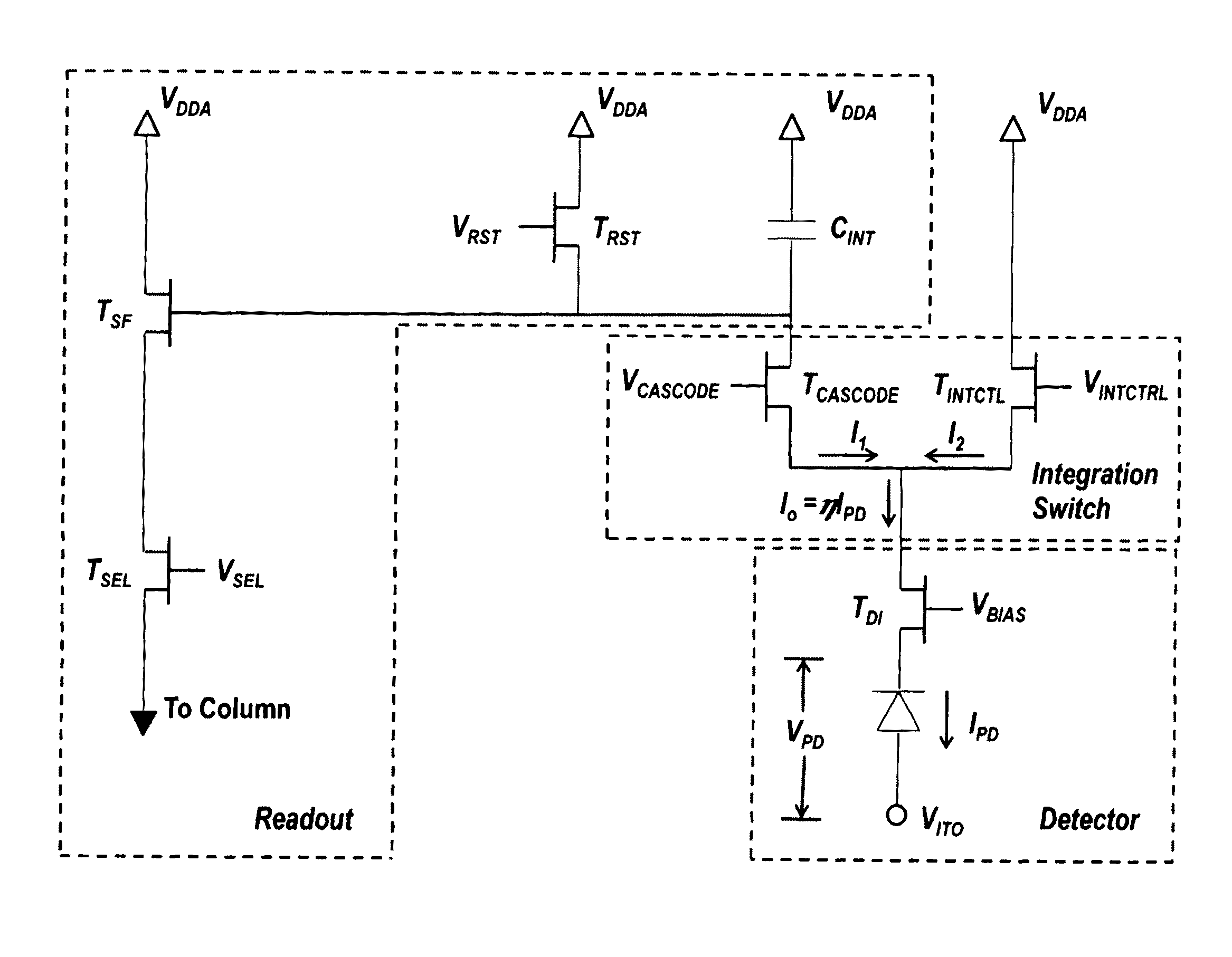
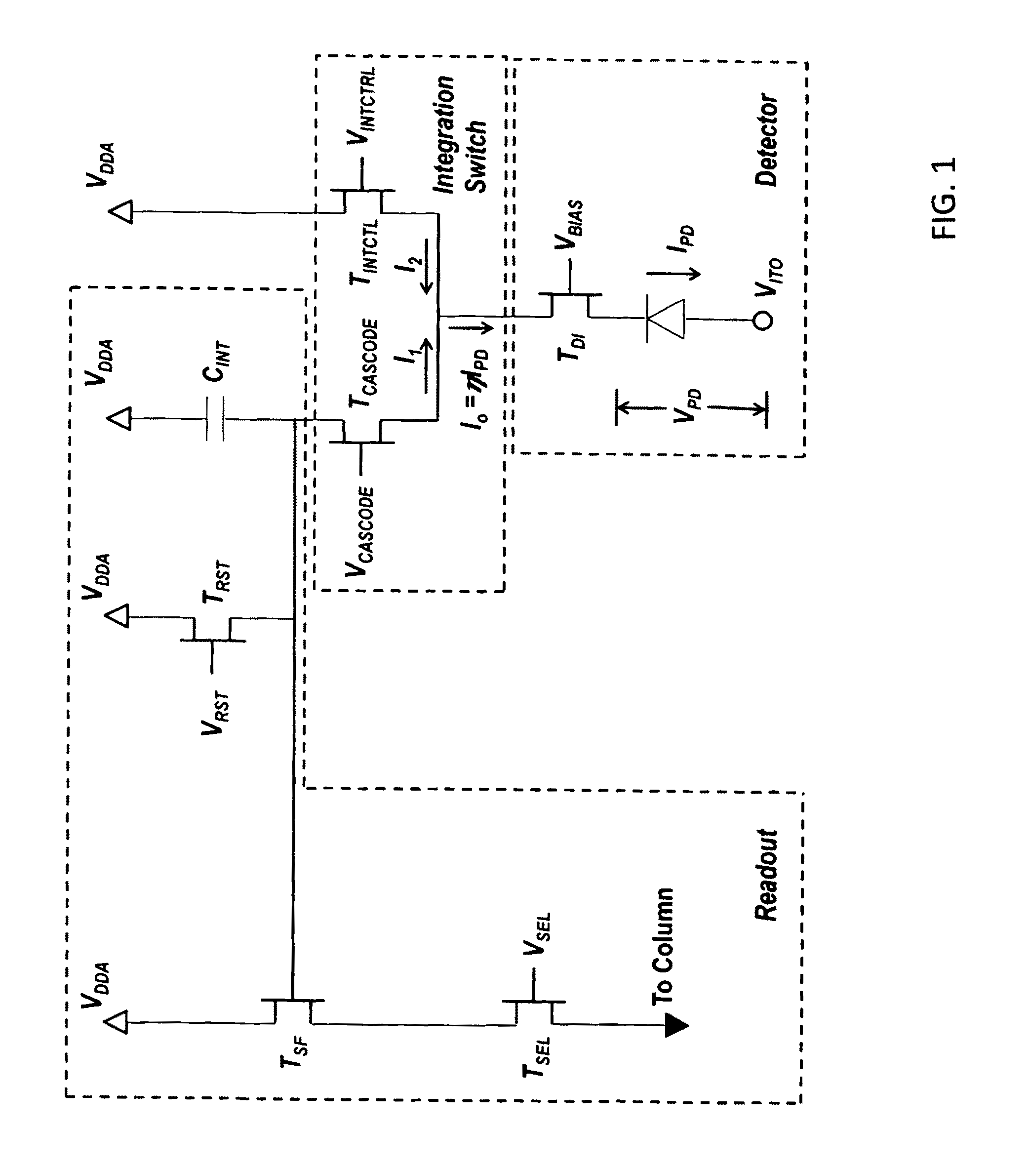
Pixel Circuit #1

[0013]Pixel Circuit #1, displayed in FIG. 1, includes the POAP photodiode, six MOSFETs, an integration capacitor, and five control lines. This circuit is designed to collect electrons (versus holes) from the photodiode. A direct injection input circuit interfaces with the POAP photodiode coating and attempts to maintain the voltage across the photodiode at a constant value. An integration switch controls the snapshot integration time. The integration capacitor collects electric charge from the photodiode. When the row readout select switch is closed, a source follower trans-impedance amplifier provides a current that is proportional to the collected charge. This current is directed to the periphery of the pixel array for amplification, digitization, and digital readout. The row reset switch, when closed, dumps the integrated charge and resets the voltage across the integration capacitor to zero. This pixel circuit can provide 1) snapshot integrate-then-read capabilit...


PUM


Abstract

Pixel circuits, capable of operating in either “snapshot” or “rolling integration” mode, and compatible with a conformal photodiode coating. Preferred embodiments of the present invention are compatible with these coating materials, as well as others, including amorphous Silicon. The preferred pixel circuits includes additional transistors not provided in prior art pixel circuits to divert leakage current away from integration nodes when not integrating, to reset the integration node, and to buffer and select the integrated voltage.

Description

CROSS-REFERENCE TO RELATED APPLICATIONS[0001]This application claims the benefit of provisional patent application Ser. No. 61 / 207,186 filed Feb. 9, 2009.BACKGROUND OF THE INVENTION[0002]Applicants and their fellow workers have developed the Photoconductor on Active Pixel (POAP) image sensor technology for the last decade. Examples of these sensors are provided in U.S. Pat. Nos. 6,730,914, 7276,749 and 7,436,038 all of which are incorporated herein by reference. They have developed an amorphous silicon (a-Si:H) p-i-n photodiode coating (0.4 micron-0.7 micron spectrum). This photodiode coating is deposited on a pixelated CMOS readout array for visible imaging applications. Applicants are presently developing a microcrystalline germanium (μc-Ge) p-i-n photodiode coating (0.4 micron-1.6 micron spectrum). This photodiode coating is deposited on a pixelated CMOS readout array for visible (VIS), near infrared (NIR) and short wave infrared (SWIR) imaging applications. U.S. Pat. No. 6,730,9...

Claims


Application Information

Patent Timeline
Patent Type & Authority Patents(United States)
IPC IPC(8): H01J40/14
CPCH04N5/3532H04N5/357H04N5/37452H01L27/14609H04N25/531H04N25/60H04N25/771
Inventor MARTIN, PETERJOHNSON, PAULSEXTON, CHRIS
Owner TREX ENTERPRISES CORP
Why Eureka
Try Eureka