Electronic-component mount substrate, electronic device, and electronic module

a technology of electronic components and mount substrates, applied in the direction of printed circuit aspects, printed circuit non-printed electric components, semiconductor/solid-state device details, etc., can solve the problems of electronic component separation or electronic component breakage, and achieve the effect of increasing electrical reliability

Active Publication Date: 2019-06-25
KYOCERA CORP
View PDF4 Cites 0 Cited by
  • Summary
  • Abstract
  • Description
  • Claims
  • Application Information

AI Technical Summary

Benefits of technology

[0004]According to an aspect of the present invention, an electronic-component mount substrate includes a substrate having a first principal surface and a second principal surface opposite to the first principal surface; a mount electrode for mounting an electronic component on the first principal surface, the mount electrode having a first slit and sandwiching the first slit; a plane electrode surrounding the mount electrode in a plan view and having a second slit; a connection electrode connecting the mount electrode with the plane electrode; and an outer electrode on the second principal surface. The connection electrode overlaps the outer electrode and an outer edge of the outer electrode surrounds the connection electrode in a perspective plan view. With this configuration, for example, when the plane electrode is connected to the outer electrode through a via conductor, transfer of heat of the via conductor by a large amount to the electronic component through the connection electrode is suppressed, and the heat is more likely transferred to the outer electrode rather than the connection electrode. Accordingly, a warp of the electronic-component mount substrate can be suppressed, and separation of the electronic component or breakage of the electronic component can be suppressed.
[0005]According to another aspect of the present invention, an electronic device includes the electronic-component mount substrate with the above-described configuration; and an electronic component mounted on the electronic-component mount substrate. Accordingly, electrical reliability is increased.
[0006]According to still another aspect of the invention, an electronic module includes the electronic device with the above-described configuration; and a module substrate with the electronic device connected thereto. Accordingly, reliability is good for a long term.

Problems solved by technology

When the via conductor is connected to the mount electrode and overlaps a mount portion for the electronic component in a perspective plan view, heat generated from the electronic component and heat generated from the via conductor when electric current flows through the via conductor may be concentrated at a center portion of the substrate, possibly resulting in separation of the electronic component or breakage of the electronic component due to a warp of the electronic-component mount substrate.

Method used


Image

  • Electronic-component mount substrate, electronic device, and electronic module
  • Electronic-component mount substrate, electronic device, and electronic module
  • Electronic-component mount substrate, electronic device, and electronic module

Examples


first embodiment

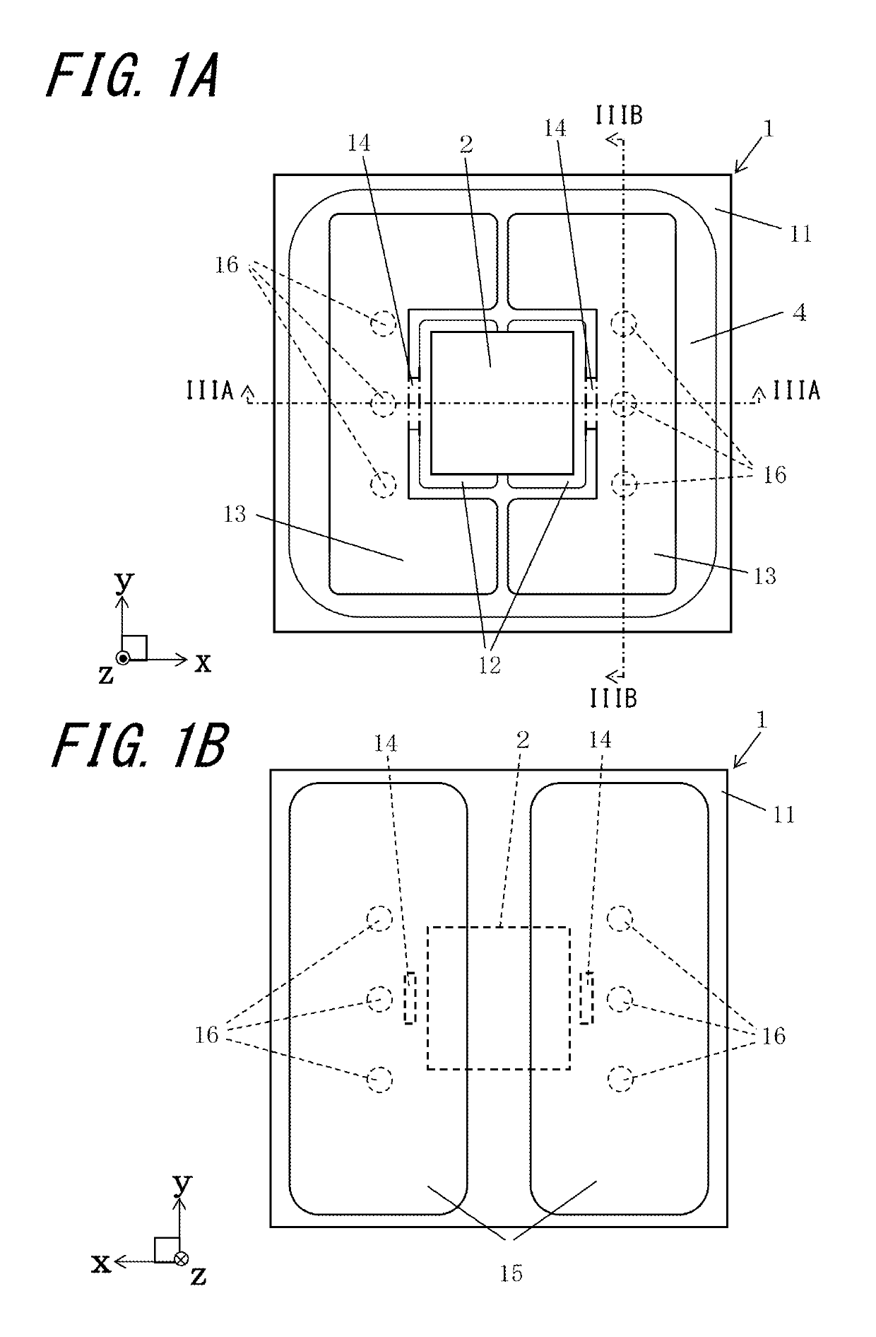
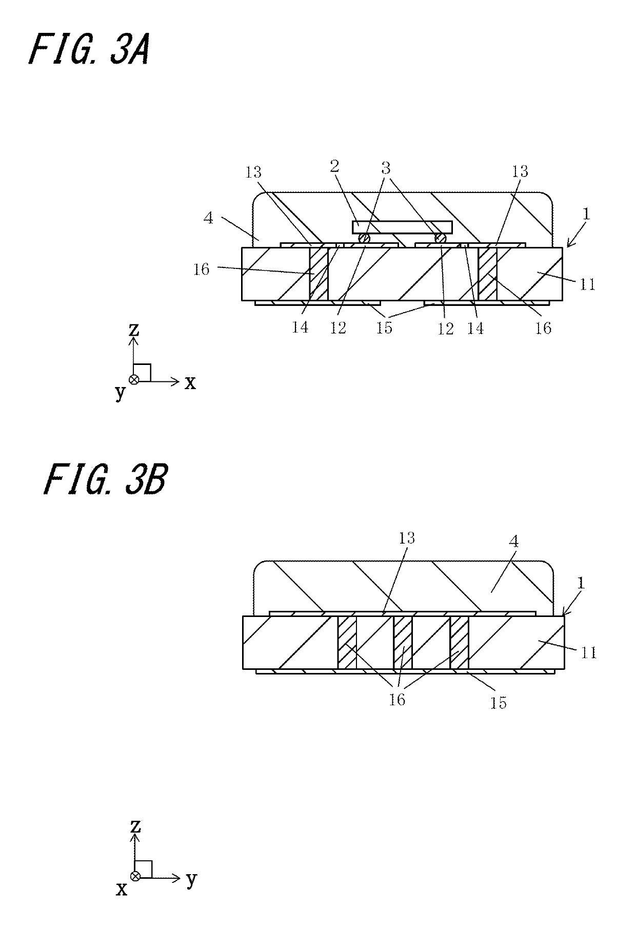
[0019]An electronic device according to a first embodiment of the present invention includes an electronic-component mount substrate 1 and an electronic component 2 on a principal surface of the electronic-component mount substrate 1 as an example illustrated in FIGS. 1A to 4. The electronic device is connected to a connection pad 51 on a module substrate 5 forming an electronic module by using a joining material 6 as the example illustrated in FIG. 4.

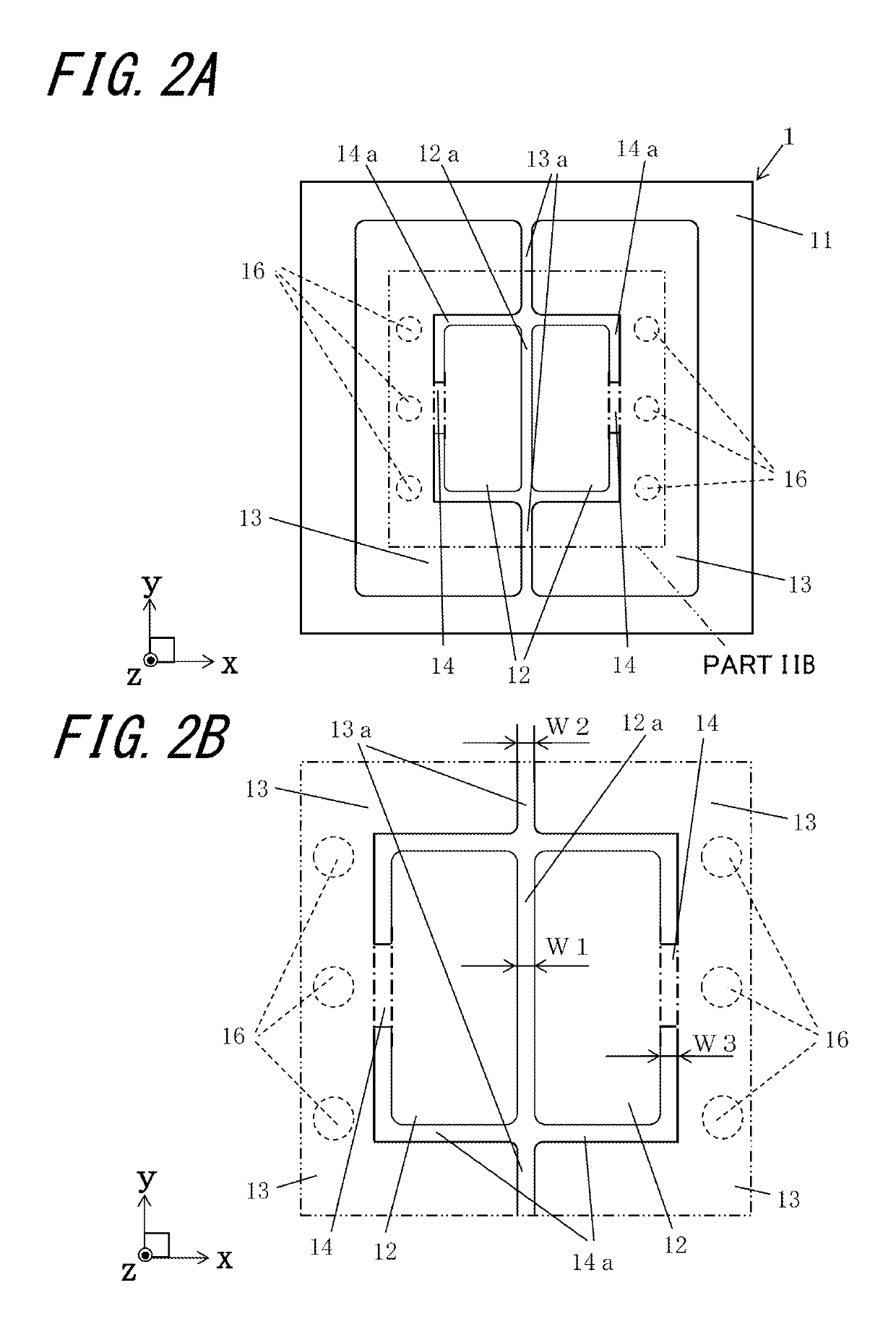
[0020]The electronic-component mount substrate 1 according to this embodiment includes a substrate 11 having a first principal surface and a second principal surface opposite to the first principal surface; a mount electrode 12 for mounting the electronic component 2 on the first principal surface, the mount electrode 12 having a first slit 12a and sandwiching the first slit 12a; a plane electrode 13 surrounding the mount electrode 12 in a plan view and having a second slit 13a; a connection electrode 14 connecting the mount electrode ...

second embodiment

[0041]An electronic device according to a second embodiment of the present invention is described next with reference to FIGS. 5A to 7B.

[0042]The electronic device according to the second embodiment of the present invention differs from the electronic device of the above-described embodiment in that the via conductor 16 is at a position separated from an imaginary line N connecting a center portion of the mount portion with the connection electrode 14 and separated from the second slit 13a.

[0043]In the example illustrated in FIGS. 5A and 6, a region where the side surface of the via conductor 16 overlaps the plane electrode 13 in a perspective plan view is indicated by broken lines. In the example illustrated in FIG. 5B, a region where the edge portion of the connection electrode 14 and the side surface of the via conductor 16 overlap the outer electrode 15 in the perspective plan view is indicated by broken lines.

[0044]The center portion of the mount portion is the center of the r...

third embodiment

[0050]An electronic device according to a third embodiment of the present invention is described next with reference to FIGS. 8A, 8B, and 9.

[0051]The electronic device according to the third embodiment of the present invention differs from the electronic device according to any of the above-described embodiments in that the connection electrode 14 includes a plurality of connection electrodes 14 that connect a single mount electrode 12 with a single plane electrode 13. In the example illustrated in FIGS. 8A and 8B, three connection electrodes 14 are between a single mount electrode 12 and a single plane electrode 13.

[0052]In the example illustrated in FIGS. 8A and 9, a region where the side surface of the via conductor 16 overlaps the plane electrode 13 in a perspective plan view is indicated by broken lines. In the example illustrated in FIG. 8B, a region where the edge portion of the connection electrode 14 and the side surface of the via conductor 16 overlap the outer electrode 1...


PUM


Abstract

An electronic-component mount substrate includes a substrate having a first principal surface and a second principal surface opposite to the first principal surface; a mount electrode for mounting an electronic component on the first principal surface, the mount electrode having a first slit and sandwiching the first slit; a plane electrode surrounding the mount electrode in a plan view and having a second slit; a connection electrode connecting the mount electrode with the plane electrode; and an outer electrode on the second principal surface. The connection electrode overlaps the outer electrode and an outer edge of the outer electrode surrounds the connection electrode in a perspective plan view.

Description

BACKGROUND OF THE INVENTION1. Field of the Invention[0001]The present invention relates to an electronic-component mount substrate, an electronic device, and an electronic module.2. Description of the Related Art[0002]An electronic-component mount substrate of related art includes a mount electrode on a first principal surface of a substrate, for mounting an electronic component; an outer electrode on a second principal surface of the substrate; and a via conductor connecting the mount electrode with the outer electrode. When an electronic device including the electronic component and the electronic-component mount substrate is joined to, for example, a module substrate, by using a joining material such as solder, the outer electrode is joined to the module substrate via the joining material such as solder (see Japanese Unexamined Patent Application Publication No. 2014-086630).[0003]In recent years, the electronic device has been requested to be advanced in function and decreased i...

Claims


Application Information

Patent Timeline
Patent Type & Authority Patents(United States)
IPC IPC(8): H05K1/18H01L23/00H05K1/14H05K1/02H05K1/11H05K3/34H01L23/31H01L25/065H05K3/30H01L23/498
CPCH05K3/3442H01L23/315H01L24/29H01L24/75H05K1/0206H05K1/111H05K1/141H05K3/3405H05K2201/10606H05K2201/09781H05K2201/049H05K3/301H01L2924/3511H01L2924/19105H01L23/3107H01L23/498H01L24/13H01L24/16H01L24/32H01L24/73H01L24/92H01L25/0655H01L2224/131H01L2224/13144H01L2224/16227H01L2224/32225H01L2224/48227H01L2224/73265H01L2224/92247H01L2924/14H01L2924/15311H01L2924/15313H01L2924/19041H01L2924/014H01L2924/00014H01L2924/00012H01L23/12H01L23/13H01L23/492H01L23/3677H01L23/49811H01L23/49827H01L23/49838H01L2924/00
Inventor MURAKAMI, KENSAKU
Owner KYOCERA CORP
Why Eureka
Try Eureka