Optical scanner, image display device, and head mounted display
a technology of image display device and optical scanner, which is applied in the direction of optical elements, television systems, instruments, etc., can solve the problems of reduced reliability, excessive etching of torsion bars, and difficult manufacturing of optical scanners, and achieve the effect of high reliability
- Summary
- Abstract
- Description
- Claims
- Application Information
AI Technical Summary
Benefits of technology
Problems solved by technology
Method used
Image
Examples
first embodiment
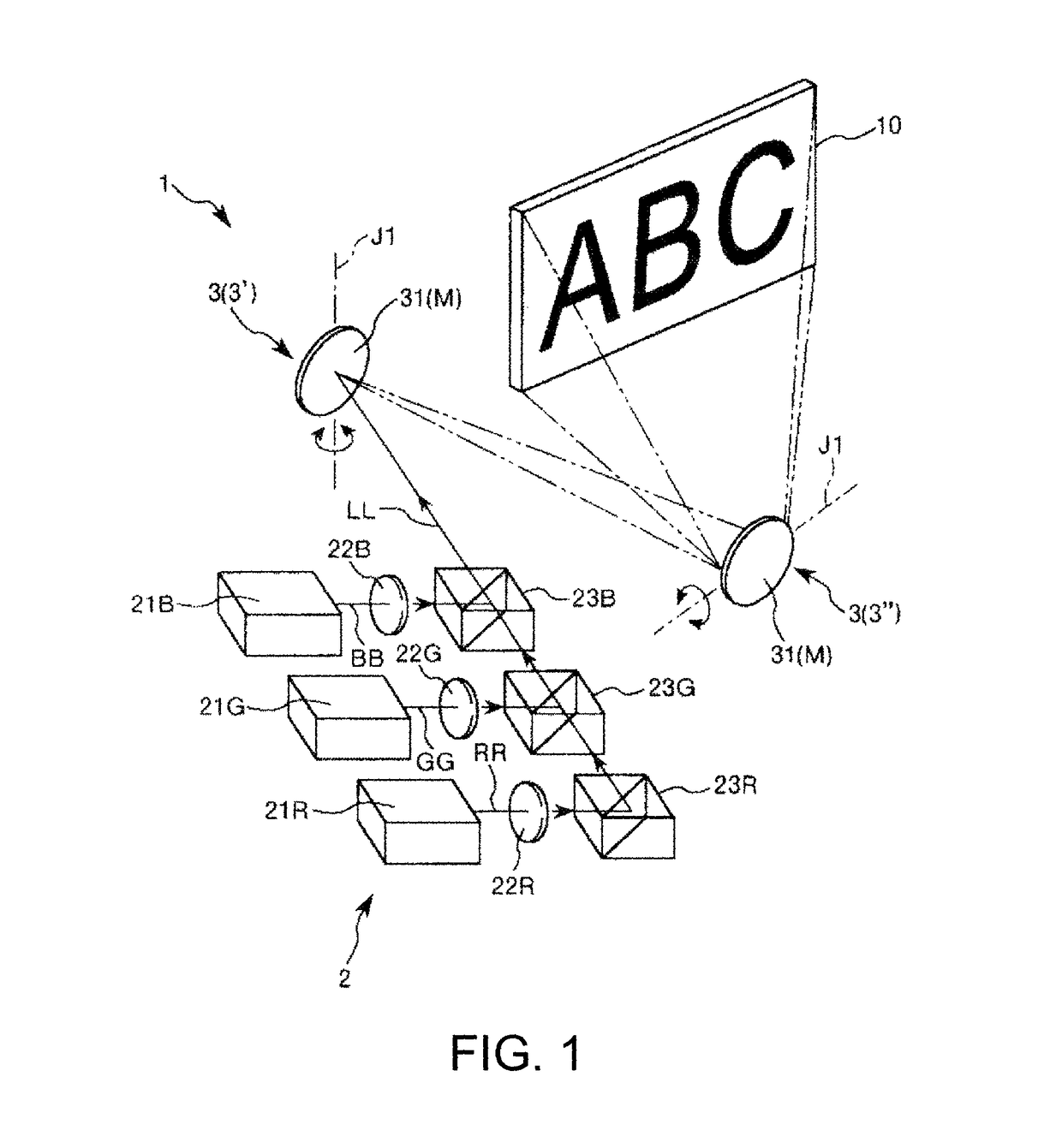
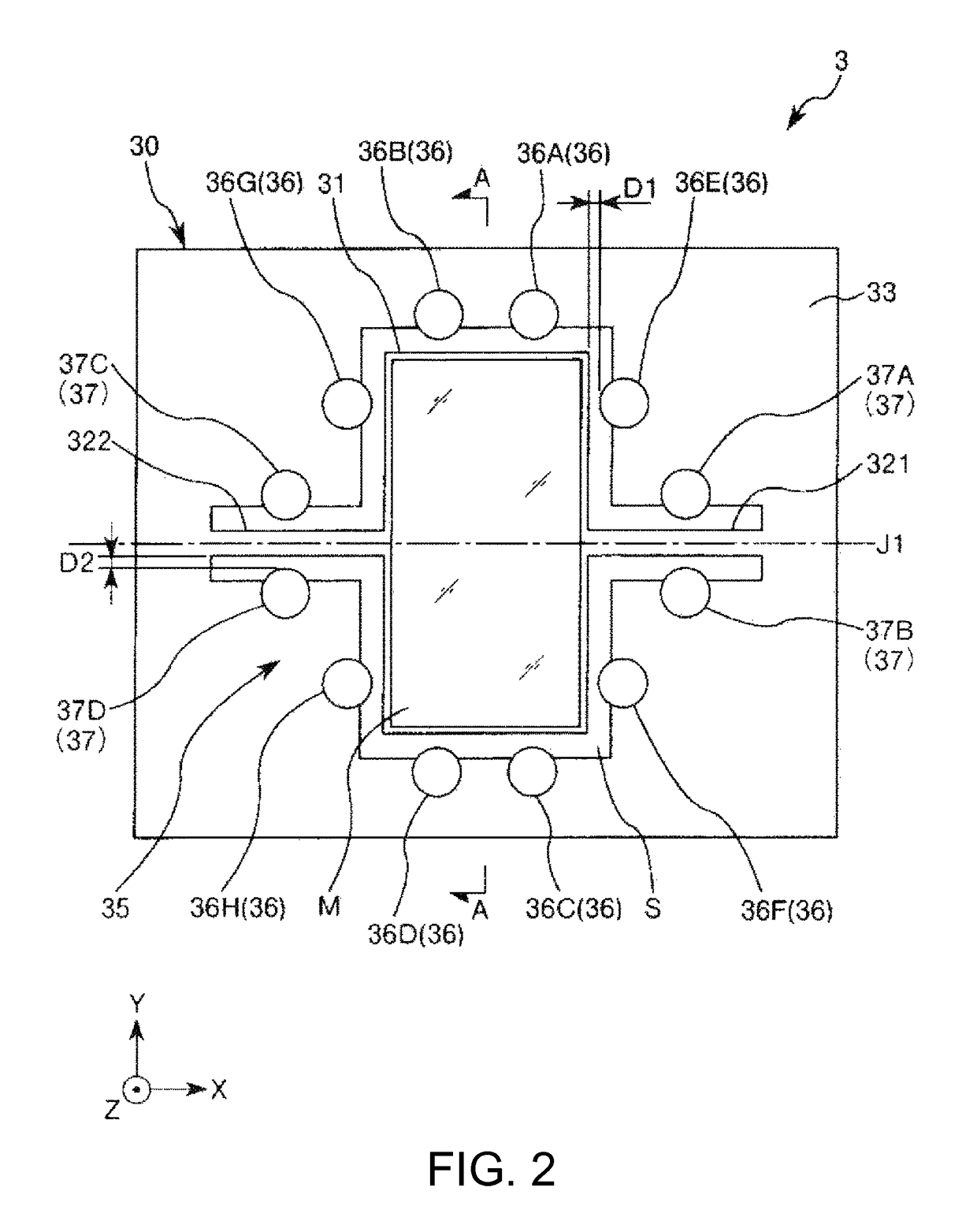
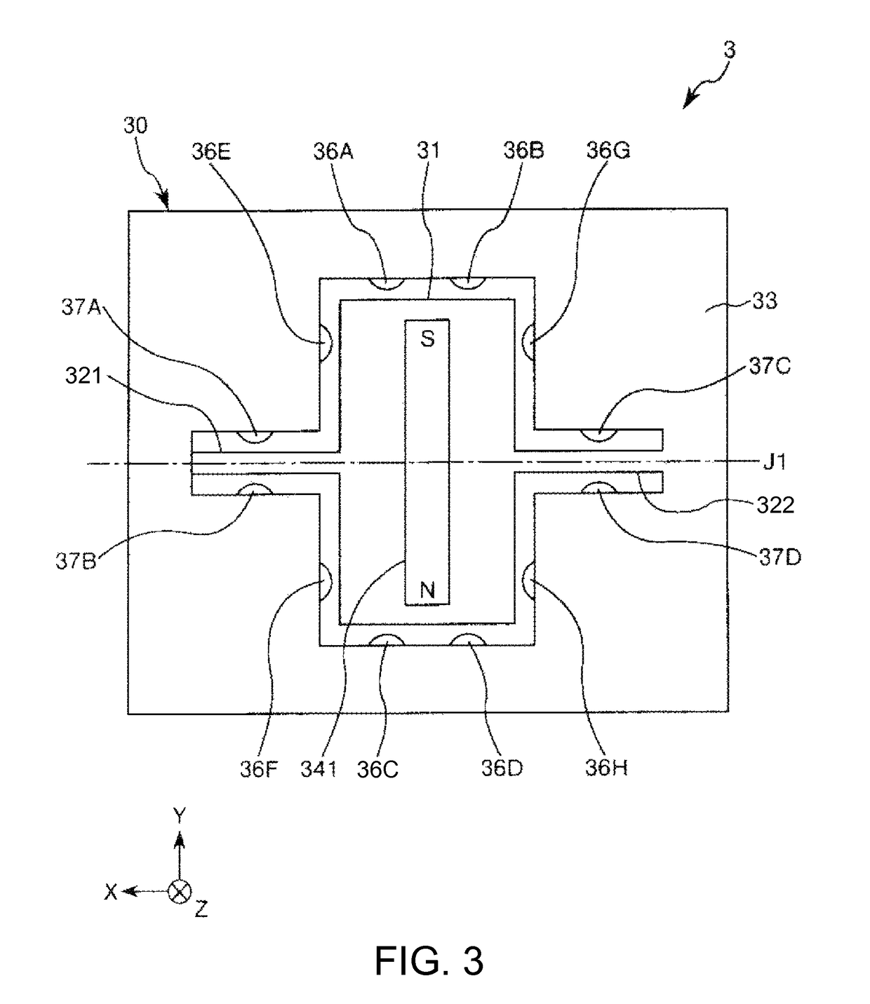
[0066]FIG. 1 is a configuration diagram showing the first embodiment of the image display device according to the invention. FIG. 2 is a top view of an optical scanner of the image display device shown in FIG. 1. FIG. 3 is a bottom view of the optical scanner shown in FIG. 2. FIG. 4 is a sectional view along A-A line in FIG. 2. FIGS. 5A and 5B show voltages applied to a coil shown in FIG. 4. FIGS. 6 and 7 are plan views for explanation of a function of a regulating member. FIGS. 8A and 8B are a plan view and a sectional view showing a movable part regulating member. FIGS. 9A and 9B are a plan view and a sectional view showing shaft part regulating members. FIGS. 10A and 10B are sectional views for explanation of a method of forming the movable part regulating member. Hereinafter, for convenience of explanation, the +Z-axis side is also referred to as “upper” and the −Z-axis side is also referred to as “lower”.
[0067]As shown in FIG. 1, an image display device 1 is a device that displ...
second embodiment
[0099]Next, the second embodiment of the image display device according to the invention will be explained.
[0100]FIG. 11 is a plan view of an optical scanner of the second embodiment of the image display device according to the invention. FIG. 12 is a sectional view along D-D line in FIG. 11.
[0101]As below, the image display device of the second embodiment will be explained with a focus on the differences from the above described embodiment and the explanation of the same items will be omitted.
[0102]The image display device of the second embodiment of the invention is the same as that of the above described first embodiment except that the configuration of the optical scanner is different. The same signs are assigned to the same configurations as those of the above described embodiment.
Optical Scanner
[0103]As shown in FIGS. 11 and 12, the optical scanner 3 of the embodiment further has a connecting portion 381 that connects the shaft part regulating members 37A, 37B and the shaft pa...
third embodiment
[0108]Next, the third embodiment of the image display device according to the invention will be explained.
[0109]FIGS. 13A and 13B are sectional views of an optical scanner of the third embodiment of the image display device according to the invention.
[0110]As below, the image display device of the third embodiment will be explained with a focus on the differences from the above described embodiments and the explanation of the same items will be omitted.
[0111]The image display device of the third embodiment of the invention is the same as that of the above described first embodiment except that the configuration of the regulating member of the optical scanner is different. The same signs are assigned to the same configurations as those of the above described embodiments.
[0112]As shown in FIGS. 13A and 13B, in the optical scanner 3 of the embodiment, the movable part regulating member 36 includes a core part 362 and a resin layer 363 covering the core part 362, and the shaft part regu...
PUM
 Abstract
Description
Claims
Application Information


