Surface gratings, photonics circuit, and method for wafer-level testing thereof

Active Publication Date: 2019-07-30
MARVELL ASIA PTE LTD
View PDF2 Cites 17 Cited by
  • Summary
  • Abstract
  • Description
  • Claims
  • Application Information

AI Technical Summary

Benefits of technology

[0006]The present invention relates to optical telecommunication techniques. More particularly, the present invention provides a surface grating for optical IO with polarization slitting

Problems solved by technology

But Internet and mobile applications continuously demand a huge amount of

Method used


Image

  • Surface gratings, photonics circuit, and method for wafer-level testing thereof
  • Surface gratings, photonics circuit, and method for wafer-level testing thereof
  • Surface gratings, photonics circuit, and method for wafer-level testing thereof

Examples


Embodiment Construction

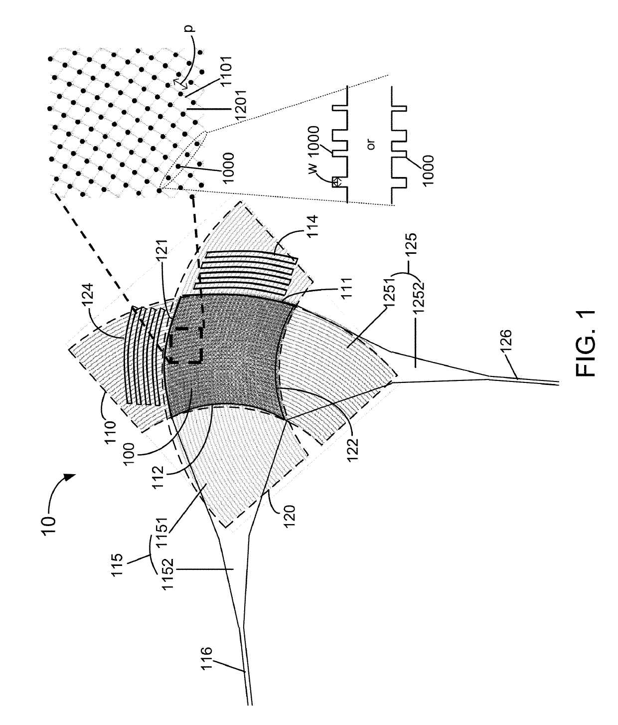
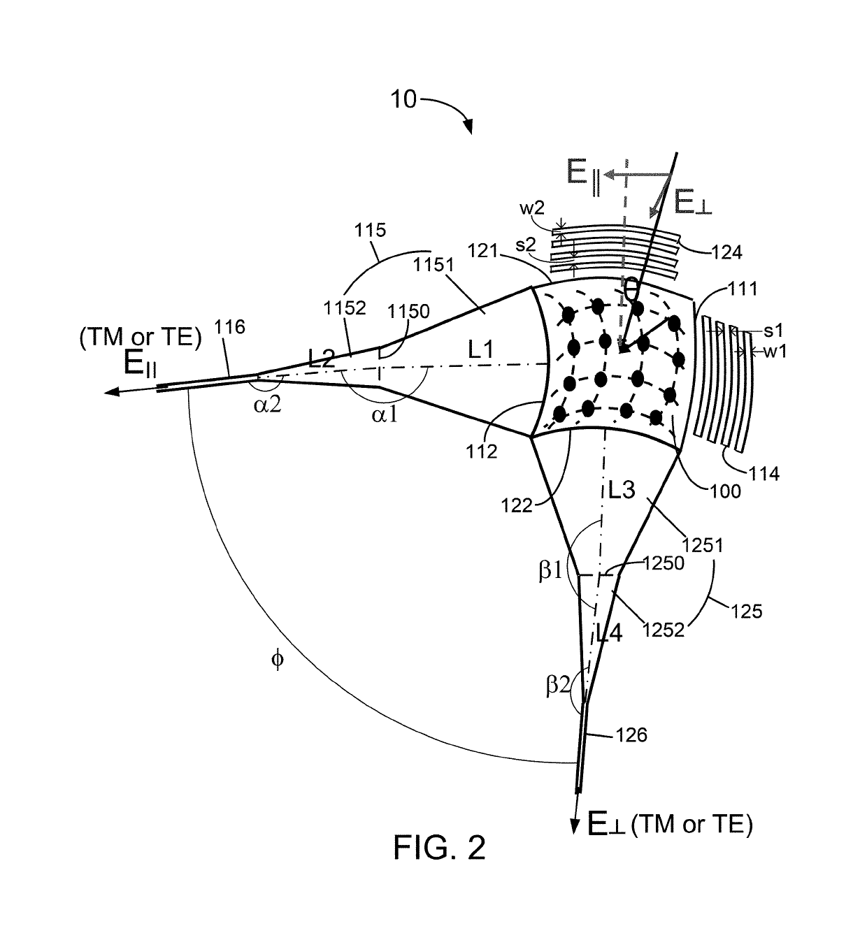
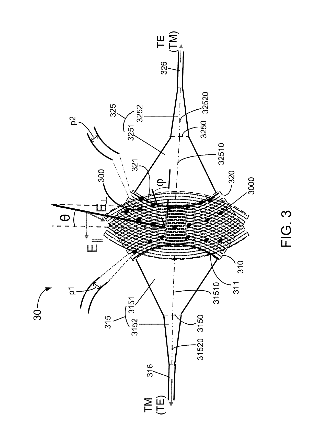
[0025]The present invention relates to optical telecommunication techniques. More particularly, the present invention provides a surface grating for optical IO with polarization splitting or diverse function for performing wafer-level testing of an array of photonics chip components on chip for high data rate optical communications, though other applications are possible.

[0026]The following description is presented to enable one of ordinary skill in the art to make and use the invention and to incorporate it in the context of particular applications. Various modifications, as well as a variety of uses in different applications will be readily apparent to those skilled in the art, and the general principles defined herein may be applied to a wide range of embodiments. Thus, the present invention is not intended to be limited to the embodiments presented, but is to be accorded the widest scope consistent with the principles and novel features disclosed herein.

[0027]In the following de...


PUM


Abstract

A surface grating coupler for polarization splitting or diverse includes a planar layer and an array of scattering elements arranged in the planar layer at intersections of a first set of concentric elliptical curves crossing with a second set of concentric elliptical curves rotated proximately 90 or 180 degrees to form a two-dimensional (2D) grating. Additionally, the grating coupler includes a first waveguide in double-taper shape and a second waveguide in double-taper shape respectively for split or diverse an incident light into the 2D grating into two output light to two output ports with a same (either TE or TM) polarization mode or one output port with TE polarization mode and another output port with TM polarization mode. The polarization diverse grating coupler is required to test multiple polarization sensitive photonics components and can be used with other single polarization grating coupler via a fiber array to perform wafer-level testing.

Description

CROSS-REFERENCE TO RELATED APPLICATIONS[0001]N / ABACKGROUND OF THE INVENTION[0002]The present invention relates to optical communication techniques. More particularly, the present invention provides a surface gratings device for optical input / output, a wafer level integrated circuit for a photonics optical system, and method of using thereof.[0003]Over the last few decades, the use of communication networks exploded. In the early days Internet, popular applications were limited to emails, bulletin board, and mostly informational and text-based web page surfing, and the amount of data transferred was usually relatively small. Today, Internet and mobile applications demand a huge amount of bandwidth for transferring photo, video, music, and other multimedia files. For example, a social network like Facebook processes more than 500 TB of data daily. With such high demands on data and data transfer, existing data communication systems need to be improved to address these needs.[0004]Prog...

Claims


Application Information

Patent Timeline
IPC IPC(8): G02B6/124G01M11/00G02B6/30G02B6/27G02B6/122G02B6/126G02B6/125G02B6/12
CPCG02B6/124G02B6/125G02B6/126G02B6/2726G02B6/1228G02B6/305G01M11/35G01M11/33G02B6/2773G02B2006/12061G02B6/34
Inventor KARIMELAHI, SAMIRAKATO, MASAKI
Owner MARVELL ASIA PTE LTD
Why Eureka
Try Eureka