Method of forming gate-all-around structures

a technology of all-around structure and gate, which is applied in the direction of basic electric elements, electrical equipment, semiconductor devices, etc., can solve the problems of increasing manufacturing and processing complexity, increasing manufacturing complexity, and not being fully satisfactory in all aspects, so as to increase the effective area of the channel, increase the channel width, and effectively control the channel

Active Publication Date: 2019-08-20
SHANGHAI INTEGRATED CIRCUIT RES & DEV CENT
View PDF1 Cites 0 Cited by
  • Summary
  • Abstract
  • Description
  • Claims
  • Application Information

AI Technical Summary

Benefits of technology

[0014]Accordingly, an objective of the present invention is to provide a simple, reliable, low-cost method of forming gate-all-around structure with high performance and gate control ability over four sides. The method is easy in process and compatible to the conventional integrated circuit planar technology, thereby solving the problems of process complexity and high cost.
[0038]Compared with the conventional method, the present invention provides a manufacturing method for gate-all-around structures which includes forming a buried gate layer on the semiconductor substrate; then forming an epitaxial layer in non-buried-gate-layer regions and planarizing the epitaxial layer so that the top surface of the epitaxial layer is at the same level with the top surface of the buried gate layer; forming a fin structure on the buried gate layer; forming a gate structure traversing and surrounding the fin structure. Since the gate structure wraps around four sides of the fin to effectively control the channel, the channel width is increased compared with the double-gate or triple gate structure, thereby increasing the effective area of the channel. The present invention solves the conventional problems like complex process and high cost without degrading the device performance. It has the advantages of simplicity, compatibility with the traditional integrated circuit planar process, low cost, and easy implementation.

Problems solved by technology

Although such scaling down of device dimensions enhances productivity and reduces production cost, it also increases manufacturing and processing complexity.
Although the FinFET devices and their manufacturing method have basically achieved expected results, they are not fully satisfactory in all aspects.
However, such structure is more complicated in manufacturing.
From above, the conventional manufacturing process for gate-all-around FinFETs is very complicated and costly, which limits the rapid development of FinFET devices with low cost and high productivity.
Accordingly, how to provide a simple, reliable, low-cost manufacturing method to form gate-all-around FinFETs with high performance is a problem to be resolved by those skilled in the art.

Method used


Image

  • Method of forming gate-all-around structures
  • Method of forming gate-all-around structures
  • Method of forming gate-all-around structures

Examples


Embodiment Construction

[0045]In order that objects, characteristics, and advantages of the present invention may be more fully understood, the embodiments of the present invention will now be described in detail hereafter with reference to the accompanying drawings. It should be appreciated by those skilled in the art that the specific embodiments disclosed might be readily utilized as a basis for modifying or designing other structures or processes for carrying out the purposes of the present invention. It should also be realized by those skilled in the art that such equivalent constructions and variations on the example embodiments described do not depart from the spirit of the invention.

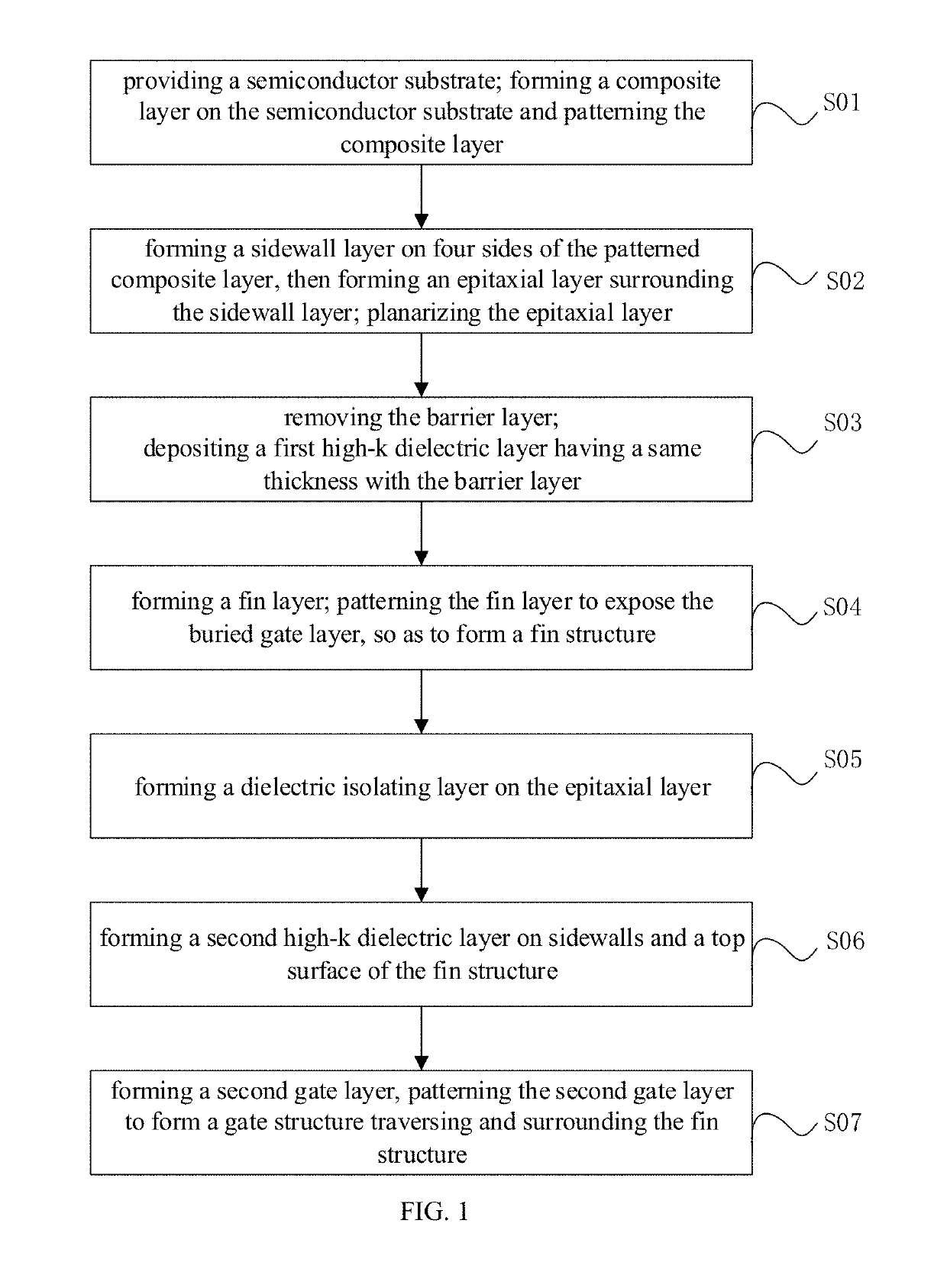
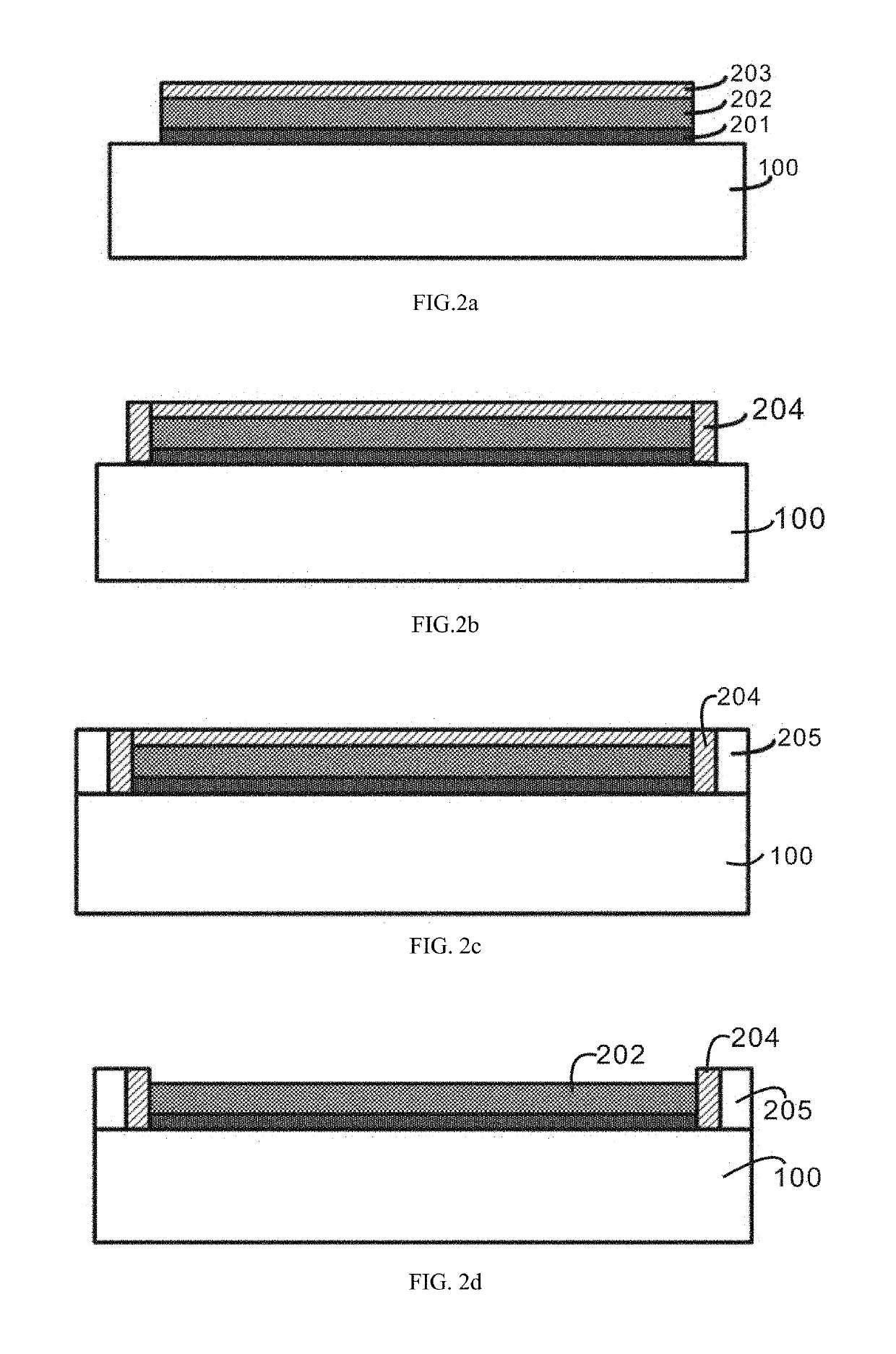
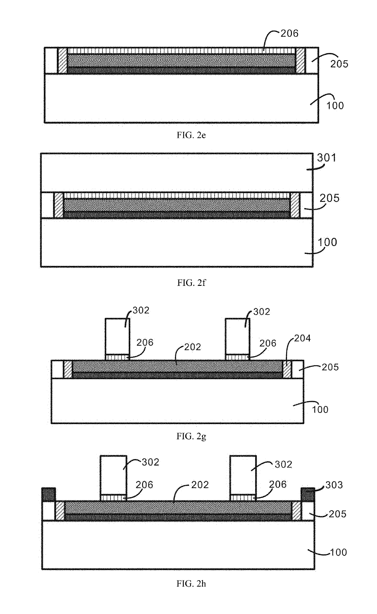
[0046]Above and additional features and advantages of embodiments of the invention will be described hereinafter. FIG. 1 is a flow chart for illustrating a method of forming gate-all-around structure according to the present invention; FIG. 2a-2j are side views of the gate-all-around structure; FIG. 3a-3j are top views ...


PUM


Abstract

A manufacturing method for gate-all-around structures in semiconductor IC manufacturing field includes forming a buried gate layer on the semiconductor substrate, forming an epitaxial layer in non-buried-gate-layer regions and planarizing the epitaxial layer so that the top surface of the epitaxial layer is at the same level with the top surface of the buried gate layer; forming a fin structure on the buried gate layer; forming a gate structure traversing and surrounding the fin structure. Since the gate structure wraps around four sides of the fin to effectively control the channel, the channel width is increased compared with the double-gate or triple gate structure, thereby increasing the effective area of the channel. The present invention solves the conventional problems like complex process and high cost without degrading the device performance. It has the advantages of simplicity, compatibility with the traditional IC planar process, low cost, and easy implementation.

Description

CROSS-REFERENCE TO RELATED APPLICATION[0001]This application claims the priority benefit of International Patent Application Serial No. PCT / CN2016 / 082308,filed May. 17, 2016, which is related to and claims the priority benefit of China patent application serial No. 201510703584.3,filed Oct. 26, 2015. The entirety of each of the above-mentioned patent applications is hereby incorporated by reference herein and made a part of this specification.FIELD OF THE INVENTION[0002]The present invention generally relates to the field of semiconductor integrated circuit manufacturing technology, and more particularly, to a method of forming gate-all-around structures.BACKGROUND OF THE INVENTION[0003]The semiconductor integrated circuit industry has experienced rapid development in the past years. With the development of the IC technology, integrated circuits are manufactured with higher functional density (numbers of devices in each chip) and smaller size (the minimum dimensions of the devices t...

Claims


Application Information

Patent Timeline
Patent Type & Authority Patents(United States)
IPC IPC(8): H01L21/28H01L21/768H01L29/423H01L21/762H01L29/66H01L29/78
CPCH01L29/66795H01L21/28H01L21/762H01L29/7855H01L29/42356H01L29/42392H01L21/76865H01L21/28158H01L29/785
Inventor HUANG, RENDONGZHONG, MIN
Owner SHANGHAI INTEGRATED CIRCUIT RES & DEV CENT
Why Eureka
Try Eureka