

Solid state imaging element and electronic device to obtain high sensitivity of light on a long wavelength side
a technology of solid-state imaging and electronic devices, which is applied in the direction of semiconductor devices, radio frequency controlled devices, electrical devices, etc., can solve the problems of reducing the sensitivity of increasing the material cost, and affecting the image quality, so as to improve the sensitivity of light absorption to light on the long wavelength side, reduce the cost of material consumption, and reduce the effect of material cos
- Summary
- Abstract
- Description
- Claims
- Application Information
AI Technical Summary
Benefits of technology
Problems solved by technology
Method used
Image

Examples
modification example 1
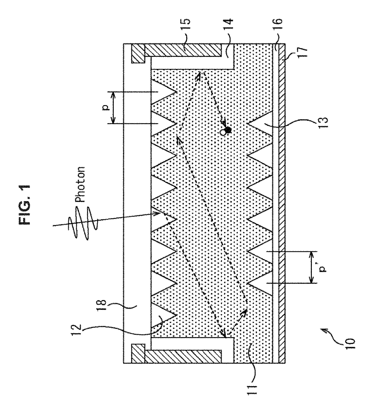
of the Solid State Imaging Element
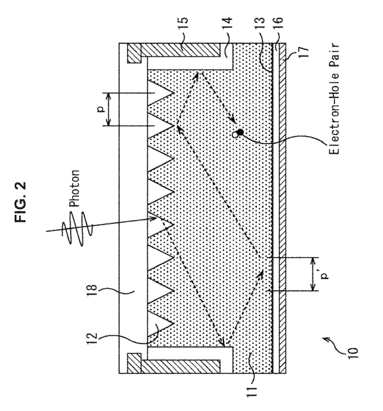
[0055]FIG. 2 is a cross-sectional view showing another example (Modification Example 1) of the configuration of the solid state imaging element 10 that is an embodiment of the present disclosure. Components in common with the configuration example shown in FIG. 1 are marked with the same reference numerals, and a description thereof is omitted as appropriate.
[0056]In Modification Example 1 shown in FIG. 2, the period of the concave-convex pattern 13 formed on the surface on the lower side of the Si layer 11 is altered to an infinitely small period.
[0057]In the case of Modification Example 1, the concave-convex patterns 12 and 13 are formed on the light receiving surface and the opposite surface to the light receiving surface of the Si layer 11, respectively. Further, the element isolation structure 14 is formed at the boundary with an adjacent pixel, and the reflecting mirror structure 17 is formed on the lower side of the Si layer 11. Thereby, inci...
modification example 2
of the Solid State Imaging Element
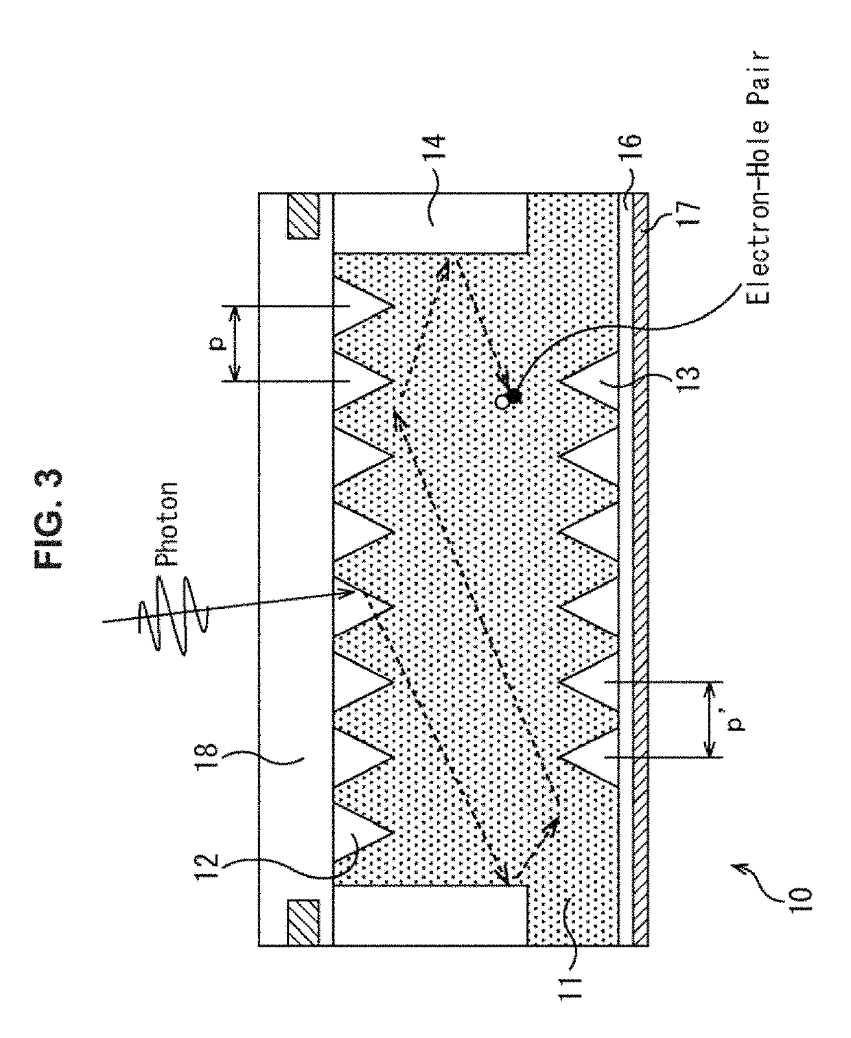
[0058]FIG. 3 is a cross-sectional view showing yet another example (Modification Example 2) of the configuration of the solid state imaging element 10 that is an embodiment of the present disclosure. Components in common with the configuration example shown in FIG. 1 are marked with the same reference numerals, and a description thereof is omitted as appropriate.
[0059]In Modification Example 2 shown in FIG. 3, the metal reflecting wall 15 is omitted from the configuration example shown in FIG. 1.
[0060]In the case of Modification Example 2, the concave-convex patterns 12 and 13 are formed on the light receiving surface and the opposite surface to the light receiving surface of the Si layer 11, respectively. Further, the element isolation structure 14 is formed at the boundary with an adjacent pixel, and the reflecting mirror structure 17 is formed on the lower side of the Si layer 11. Thereby, incident light is likely to repeat reflection in the Si l...
modification example 3
of the Solid State Imaging Element
[0061]FIG. 4 is a cross-sectional view showing yet another example (Modification Example 3) of the configuration of the solid state imaging element 10 that is an embodiment of the present disclosure. Components in common with the configuration example shown in FIG. 1 are marked with the same reference numerals, and a description thereof is omitted as appropriate.
[0062]In Modification Example 3 shown in FIG. 4, the metal reflecting wall 15 and the reflecting mirror structure 17 are omitted from the configuration example shown in FIG. 1.
[0063]In the case of Modification Example 3, the concave-convex patterns 12 and 13 are formed on the light receiving surface and the opposite surface to the light receiving surface of the Si layer 11, respectively. Further, the element isolation structure 14 is provided at the boundary with an adjacent pixel. Thereby, incident light is likely to repeat reflection in the Si layer 11, and the transmission of light from t...
PUM
 Abstract
Description
Claims
Application Information