Method of writing data to a memory device and reading data from the memory device

a memory device and data technology, applied in the direction of program/content distribution protection, unauthorized memory use protection, instruments, etc., can solve the problems of inconvenient approach and threat of interfering with a system on a chip (soc) with an external memory devi

Active Publication Date: 2019-11-12
SIEMENS AG
View PDF8 Cites 0 Cited by
  • Summary
  • Abstract
  • Description
  • Claims
  • Application Information

AI Technical Summary

Benefits of technology

[0011]Moreover, it is advantageous if the data is masked with the error corrected PUF response using the XOR operator, and if the data is revealed out of masked data with the error corrected PUF response using an XOR operator. Such a data transformation is fast and needs little computing power.

Problems solved by technology

Generally, an interaction of a system on chip (SoC) with an external memory device constitutes threats.
In some circumstances, however, this approach is not the right choice.

Method used


Image

  • Method of writing data to a memory device and reading data from the memory device
  • Method of writing data to a memory device and reading data from the memory device

Examples


Embodiment Construction

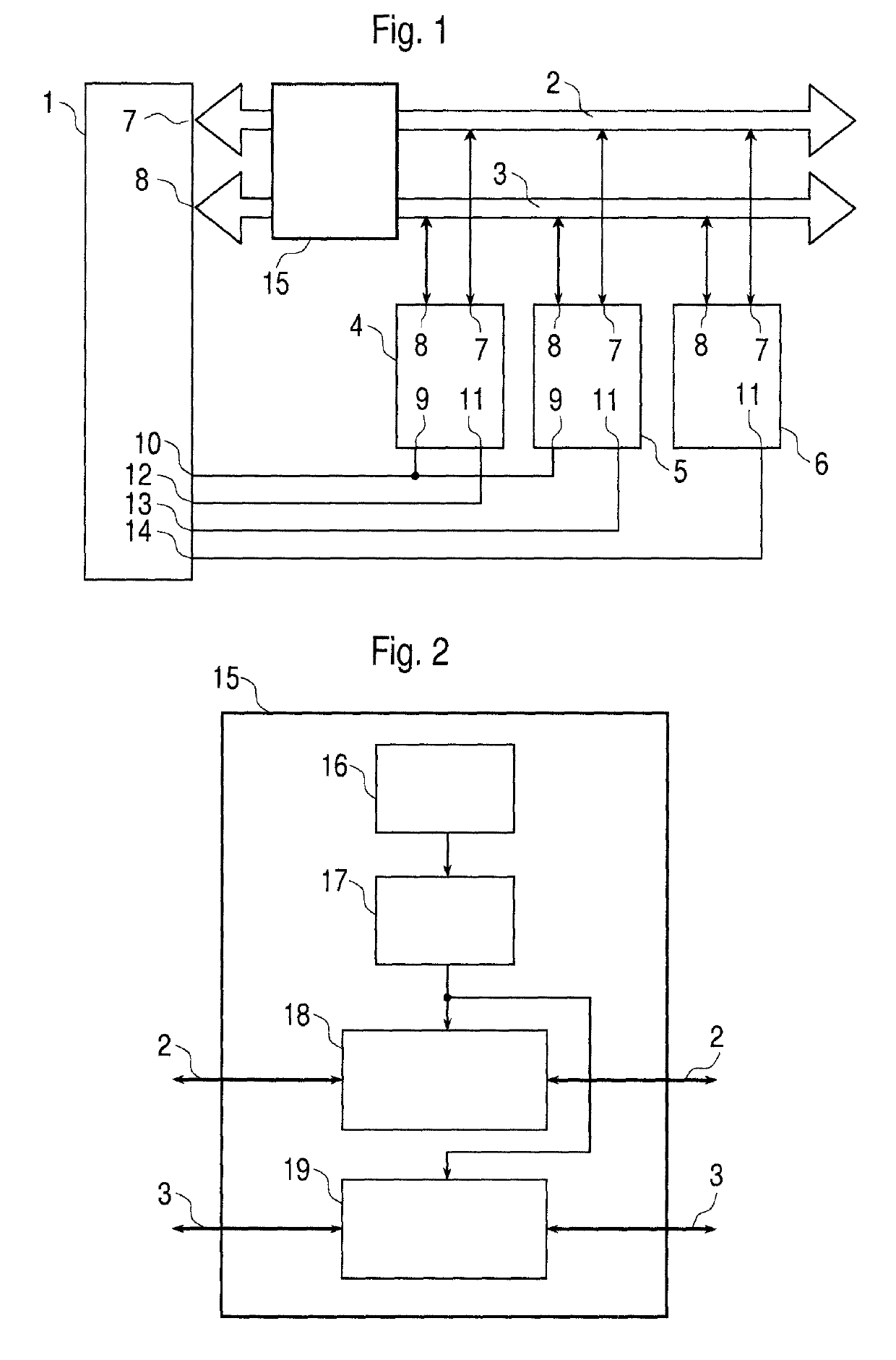
[0023]FIG. 1 shows a system on chip (SoC) with a memory controller 1 that is connected to an address bus 2 and a data bus 3. Via theses busses 2, 3, addresses and data are exchanged with various memory devices 4, 5, 6, such as RAM 4, rewritable memory 5 or ROM 6. For this purpose the memory controller 1 and the memory devices 4, 5, 6 comprise address connections 7 and data connections 8.

[0024]The RAM 4 and the rewritable memory 5 comprise R / W′-inputs 9, which are connected to a corresponding output 10 of the memory controller 1. Additionally, each memory device 4, 5, 6 comprises a CE-input 11 that is respectively connected to a corresponding CS-output 12, 13, 14 of the memory controller 1.

[0025]The memory controller 1 is responsible for accessing the external memories 4, 5, 6 attached to the SoC. The memory controller 1 sets the address on the address bus 2 and reads or writes the data via data bus 3.

[0026]Adjacent to the memory controller 1 the inventive obfuscation module 15 is co...


PUM


Abstract

A method of writing data to a memory device and reading data from the memory device includes issuing a challenge to a PUF device during a power-up process in order to derive a PUF response, error correcting the PUF response, providing delinearized addresses via a delinearization algorithm to the memory device using the error corrected PUF response, masking data, which is written to the memory device, via a masking module using the error corrected PUF response, de-masking data, which is read from the memory device, via the masking module (19) using the error corrected PUF response; and performing a check-sum verification of read data such that address delinearization and data masking are used together to obfuscate the memory content.

Description

CROSS-REFERENCE TO RELATED APPLICATIONS[0001]This is a U.S. national stage of application No. PCT / EP2016 / 050667 filed 14 Jan. 2016, and claims priority to European application No. 15464002 filed Jan. 15, 2015, the content of which is incorporated herein by reference in its entirety.BACKGROUND OF THE INVENTION1. Field of the Invention[0002]The invention relates to a method of writing data to a memory device and reading data from the memory device, and to a system on chip for implementing the method.2. Description of the Related Art[0003]Generally, an interaction of a system on chip (SoC) with an external memory device constitutes threats. In order to avoid security attacks, such as sniffing, the memories need to be protected.[0004]A common solution to provide protection is cryptography. In some circumstances, however, this approach is not the right choice. An alternative solution is address obfuscation. US2009 / 0327709-A1 discloses a method of address obfuscation, which is simple to a...

Claims


Application Information

Patent Timeline
Patent Type & Authority Patents(United States)
IPC IPC(8): G06F21/14G09C1/00G06F12/14H04L9/32G06F21/75G06F21/12
CPCG06F12/1408G09C1/00G06F21/14H04L9/3278G06F21/123G06F21/75H04L2209/12
Inventor PITU, CIPRIAN-LEONARD
Owner SIEMENS AG
Why Eureka
Try Eureka