
Solar cell, method for manufacturing same and solar cell module

a technology of solar cells and solar cells, applied in the direction of basic electric elements, electrical equipment, semiconductor devices, etc., can solve the problems of high resistivity, high material cost, shadow loss, etc., and achieve the effect of excellent light collection efficiency

Active Publication Date: 2020-02-18
KANEKA CORP
View PDF22 Cites 0 Cited by
  • Summary
  • Abstract
  • Description
  • Claims
  • Application Information

AI Technical Summary

Benefits of technology

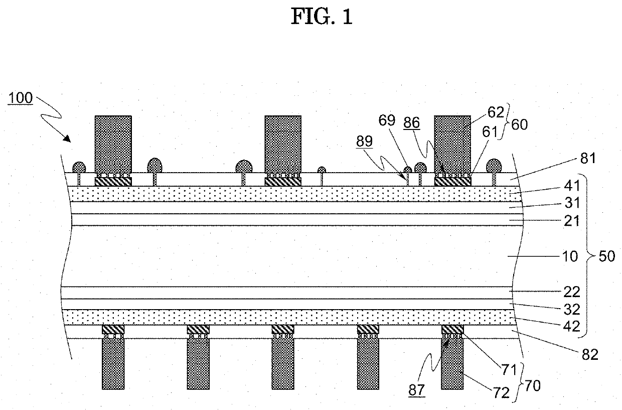
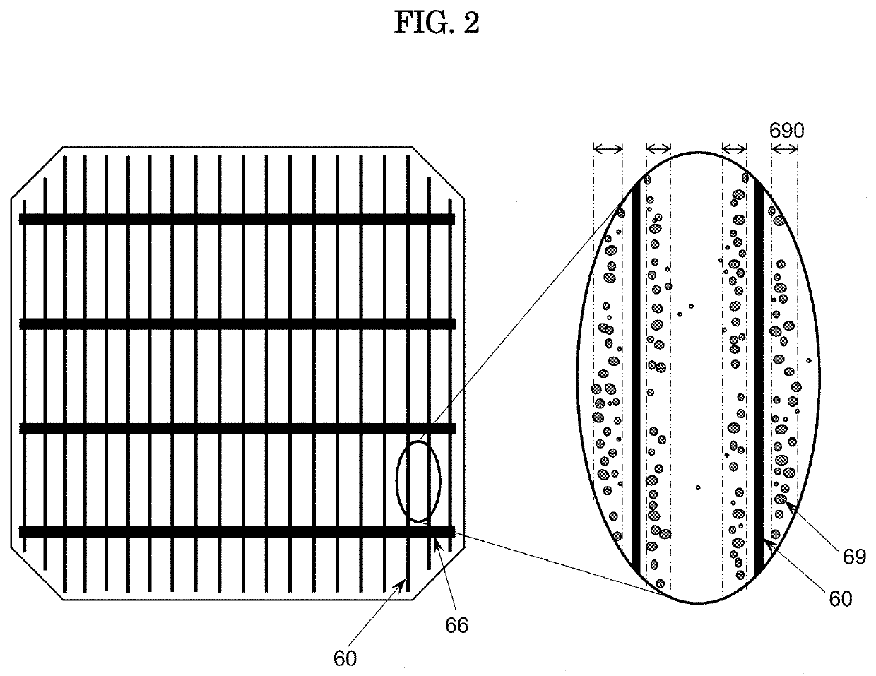
[0021]In the solar cell of the present invention, light reflected on the finger electrodes on the light-receiving side can be scattered on the isolated plating metal layer pieces to enter into the photoelectric conversion section. Thus, the solar cell is excellent in light collection efficiency.

Problems solved by technology

Light that is irradiated on regions where the metal collecting electrodes are formed is reflected on or absorbed by the metal collecting electrodes to cause shadowing loss.
The collecting electrode formed by using silver paste contains a resin material, so that it is high in resistivity and high in material costs.

Method used


Image

  • Solar cell, method for manufacturing same and solar cell module
  • Solar cell, method for manufacturing same and solar cell module
  • Solar cell, method for manufacturing same and solar cell module

Examples


example 1

(Texture Formation on Silicon Substrate Surface)

[0093]An n-type single-crystalline silicon substrate having a light receiving surface with a (100) plane orientation and having a thickness of 200 μm was washed in acetone, immersed in a 2 wt % HF aqueous solution for 5 minutes to remove a silicon oxide layer on a surface, and rinsed twice with ultra-pure water. Washed silicon substrate was immersed for 15 minutes in a 5 / 15 wt % KOH / isopropyl alcohol aqueous solution held at 75° C. to perform anisotropic etching. Thereafter, the substrate was immersed in a 2 wt % HF aqueous solution for 5 minutes, rinsed twice with ultra-pure water, and then dried at ambient temperature. Surfaces of the silicon substrate were observed with an AFM to confirm that quadrangular pyramid-like textured structures having an exposed (111) surface were formed on each of the front and back surfaces The arithmetic mean roughness thereof was 2100 nm.

[0094](Formation of Silicon-Based Thin-Films)

[0095]The texture-fo...


PUM

PropertyMeasurementUnit
thicknessaaaaaaaaaa
diameteraaaaaaaaaa
thicknessaaaaaaaaaa

Abstract

The solar cell includes a plurality of light-receiving-side finger electrodes on a light-receiving surface of a photoelectric conversion section having a semiconductor junction. The light-receiving surface of the photoelectric conversion section is covered with a first insulating layer. Each light-receiving-side finger electrodes include: a first metal seed layer provided between the photoelectric conversion section and the first insulating layer; and a first plating metal layer being conduction with the first metal seed layer through openings formed in the first insulating layer. The solar cell includes an isolated plating metal layer pieces contacting neither the light-receiving-side finger electrodes nor the back-side finger electrodes. On the surface of the first insulating layer, an isolated plating metal crowded region is present in a form of a band-shape extending parallel to an extending direction of the light-receiving-side finger electrodes.

Description

CROSS REFERENCE TO RELATED APPLICATION[0001]This present application is a national stage filing under 35 U.S.C. § 371 of PCT application number PCT / JP2016 / 050406 filed on Jan. 7, 2016 which is based upon and claims the benefit of priority to Japanese Patent Application No. 2015-001329 filed on Jan. 7, 2015 in the JPO (Japanese Patent Office). The disclosures of the above-listed applications are hereby incorporated by reference herein in their entirety.TECHNICAL FIELD[0002]The invention relates to solar cell, manufacturing method thereof and solar cell module.BACKGROUND ART[0003]In a solar cell, carriers (electrons and holes) generated by light irradiation to a photoelectric conversion section composed of a semiconductor junction are extracted to an external circuit to generate electricity. Metal electrodes are provided on front surface and back surface of the photoelectric conversion section of the solar cell for efficiently extracting carriers generated at the photoelectric convers...

Claims


Application Information

Patent Timeline
Patent Type & Authority Patents(United States)
IPC IPC(8): H01L31/0216H01L31/0747H01L31/0224H01L31/054
CPCH01L31/02168H01L31/0543H01L31/022425H01L31/0747H01L31/022466H01L31/02164H01L31/022433Y02E10/52
Inventor YOSHIKAWA, KUNTAADACHI, DAISUKETERASHITA, TORUHIRAISHI, MASAFUMI
Owner KANEKA CORP
Learn More