Solar cell module and method for manufacturing same

a solar cell and module technology, applied in the field of solar cell modules, can solve the problems of insufficient power generation efficiency of modules, achieve the effects of suppressing the deterioration of module characteristics, small shading area, and easy preparation

Active Publication Date: 2020-03-17
KANEKA CORP
View PDF24 Cites 0 Cited by
  • Summary
  • Abstract
  • Description
  • Claims
  • Application Information

AI Technical Summary

Benefits of technology

[0035]According to the present invention, a solar cell module with a small shading area can be easily prepared by cleaving a solar cell having a crystalline silicon substrate to a predetermined size, and stacking the solar cells after cleavage. In the present invention, deterioration of module characteristics, which may be caused in the cleaved surface, can be suppressed by stacking solar cells in such a manner that the cleaved surface of a lower solar cell provides a shading section. Further, by stacking solar cells together with an insulating member provided on the cleaved surface-side periphery of the solar cell, damage to the solar cell, which is caused from the cleaved surface, can be suppressed with the insulating member acting as a buffer material. As a result, deterioration of module conversion efficiency and reliability can be suppressed.

Problems solved by technology

However, in a solar cell module prepared in this way, the gap section is a region which does not contribute to power generation, and therefore module power generation efficiency is insufficient.

Method used


Image

  • Solar cell module and method for manufacturing same
  • Solar cell module and method for manufacturing same
  • Solar cell module and method for manufacturing same

Examples


embodiment 1

[0098]First, one example of a method for manufacturing a solar cell module according to embodiment 1 will be described with reference to FIGS. 7A and 7B and FIGS. 8A and 8B.

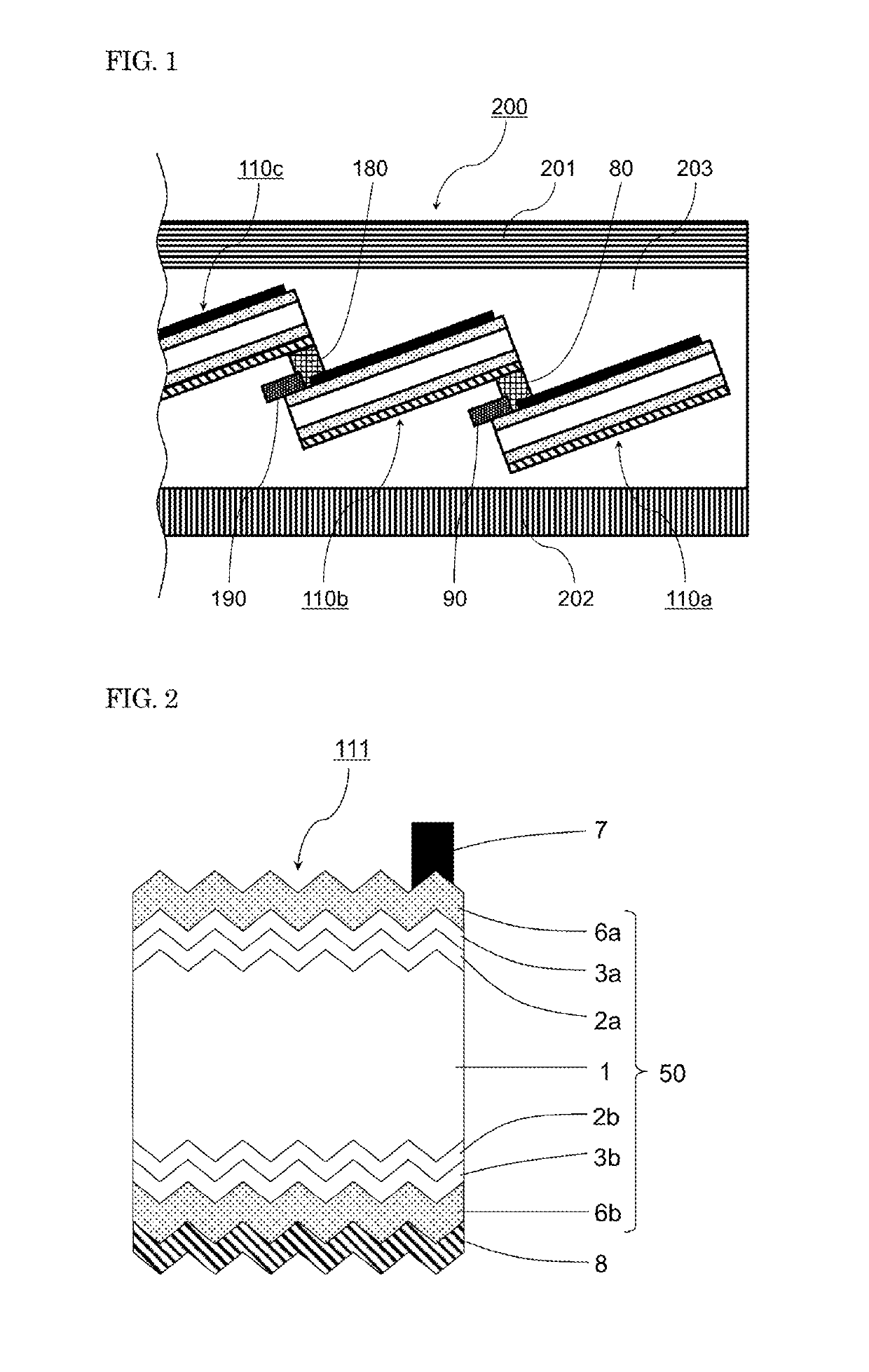
[0099]As shown in FIG. 7A, a solar cell 100 is provided and the solar cell 100 is cleaved into two parts. The solar cell 100 has a photoelectric conversion section 150 that includes a single-crystalline silicon substrate of first conductivity-type, collecting electrodes 17 and 27 provided on a light-receiving surface of the photoelectric conversion section 150, and a back electrode (not illustrated) provided on a back surface of the photoelectric conversion section 150. The collecting electrode 17 includes a finger electrode 171 and a bus bar electrode 172, and the collecting electrode 27 includes a finger electrode 271 and a bus bar electrode 272.

[0100]The single-crystalline silicon substrate is prepared by slicing a silicon ingot to a predetermined thickness using a wire saw etc., the silicon ingot being prepar...

embodiment 2

[0133]FIG. 10 schematically shows embodiment 2. In FIG. 10, an insulating member 91 is also provided on a collecting electrode 17 of a first solar cell 110a.

[0134]In embodiment 2, the area of the insulating member at the stacked section can be increased, and therefore a higher buffer effect can be expected.

embodiment 3

[0135]FIG. 11 schematically shows embodiment 3. In FIG. 11, an insulating member 92 is in contact with a back electrode 28 of a second solar cell 110b. Preferably, a double-side tape made of polyimide etc. is used as the insulating member 92.

[0136]In embodiment 3, not only the effect described in embodiment 1 can be obtained, but also misregistration at the time of superimposing solar cells on each other can be suppressed. As a result, a poor external appearance that may be caused by misregistration of solar cells, and associated deterioration of module performance can be suppressed.

[0137]The width (length represented by W3 in FIG. 11) of the insulating member 92 that is in contact with the back electrode 28 of the second solar cell 110b is not particularly limited. When the insulating member 92 is a double-sided tape, the width of the insulating member 92 is preferably 0.5 mm or more from the viewpoint of adhesion. The width of the insulating member 92 is preferably 5 mm or less fr...


PUM

PropertyMeasurementUnit
thicknessaaaaaaaaaa
thicknessaaaaaaaaaa
pressureaaaaaaaaaa

Abstract

In the solar cell module, a first solar cell and a second solar cell are stacked together with an electroconductive member interposed therebetween, such that a cleaved surface-side periphery on a light-receiving surface of the first solar cell overlaps a periphery on a back surface of the second solar cell. The first solar cell and the second solar cell each have: photoelectric conversion section including a crystalline silicon substrate; collecting electrode; and back electrode. At a section where the first solar cell and the second solar cell are stacked, the collecting electrode of the first solar cell and the back electrode of the second solar cell are electrically connected to each other by coming into contact with the electroconductive member. An insulating member is provided on a part of the cleaved surface-side periphery on the light-receiving surface of the first solar cell, where the collecting electrode is not provided.

Description

TECHNICAL FIELD[0001]The invention relates to solar cell module and method for manufacturing thereof.BACKGROUND ART[0002]Since energy issues and global environmental issues are becoming more serious, solar cells are receiving more attention as an alternative energy source for replacing fossil fuels. In the solar cell, carriers (electrons and holes) generated by photo irradiation to a photoelectric conversion section composed of a semiconductor junction or the like are extracted to an external circuit to generate electricity. Solar cell having a collecting electrode on the photoelectric conversion section is utilized for efficiently extracting carriers generated at the photoelectric conversion section to the external circuit.[0003]Solar cells are classified broadly into thin-film-based solar cells in which a photoelectric conversion layer is deposited on a glass substrate or an electroconductive substrate, and crystalline solar cells using a single-crystalline silicon substrate or a ...

Claims


Application Information

Patent Timeline
Patent Type & Authority Patents(United States)
IPC IPC(8): H01L31/02H01L31/077H01L31/20H01L31/0352H01L31/0216H01L31/05H01L31/0224H01L31/043H01L31/042
CPCH01L31/022433H01L31/02167H01L31/035281H01L31/077H01L31/0201H01L31/043H01L31/20H01L31/022466H01L31/0504Y02E10/50Y02E10/547
Inventor NAKANO, KUNIHIROYOSHIKAWA, KUNTATERASHITA, TORUHIRAISHI, MASAFUMIYAMAMOTO, KENJI
Owner KANEKA CORP
Why Eureka
Try Eureka