Unlock instant, AI-driven research and patent intelligence for your innovation.

Manufacturing method for TFT array substrate and TFT array substrate

a manufacturing method and technology of tft array substrate, applied in the field of display, can solve the problems of affecting the carrier mobility of the polysilicon layer, affecting the quality of the display device, etc., and achieve the effect of improving the carrier mobility of the tft device, reducing the number of grain boundaries, and increasing the grain siz

Active Publication Date: 2020-03-24
TCL CHINA STAR OPTOELECTRONICS TECH CO LTD
View PDF7 Cites 0 Cited by
  • Summary
  • Abstract
  • Description
  • Claims
  • Application Information

AI Technical Summary

Benefits of technology

[0005]The object of the present invention is to provide a manufacturing method for TFT array substrate, able to increase the size of crystal grains in the active layer, reduce the number of grain boundaries, improve the carrier mobility of TFT device, and improve the electrical properties of the TFT device.
[0006]Another object of the present invention is to provide a TFT array substrate, having large size of crystal grains in the active layer, less number of grain boundaries, higher carrier mobility of TFT device, and better electrical properties of the TFT device.
[0032]The present invention provides the following advantages: the manufacturing method for TFT array substrate provided by the present invention forms a first buffer layer on the substrate; the first buffer layer is disposed with a plurality of arc protrusions or a plurality of arc recesses; then an a-Si layer is formed on the second buffer layer which is formed on the first buffer layer; in the process of forming a polysilicon layer by performing ELA on the a-Si layer, the arc protrusions or the arc recesses can change the optical path of the laser to form an energy gradient in the a-Si layer, so as to increase the grain size in the formed polysilicon layer, reduce the number of grain boundaries, improve the carrier mobility of the TFT device, and improve the electrical properties of the TFT device. The active layer of the TFT array substrate provided by the present invention has a large crystal grain size and a small number of grain boundaries, and the TFT device has high carrier mobility and good electrical properties.

Problems solved by technology

The performance of the TFT array substrate greatly affects the quality of the display device.
Therefore, the starting point and direction of crystallization in the current amorphous silicon layer are disordered, resulting in small grain size and many boundaries between crystal grains in recrystallization of the polysilicon layer, which affect the carrier mobility of the polysilicon layer.

Method used


Image

  • Manufacturing method for TFT array substrate and TFT array substrate
  • Manufacturing method for TFT array substrate and TFT array substrate
  • Manufacturing method for TFT array substrate and TFT array substrate

Examples


first embodiment

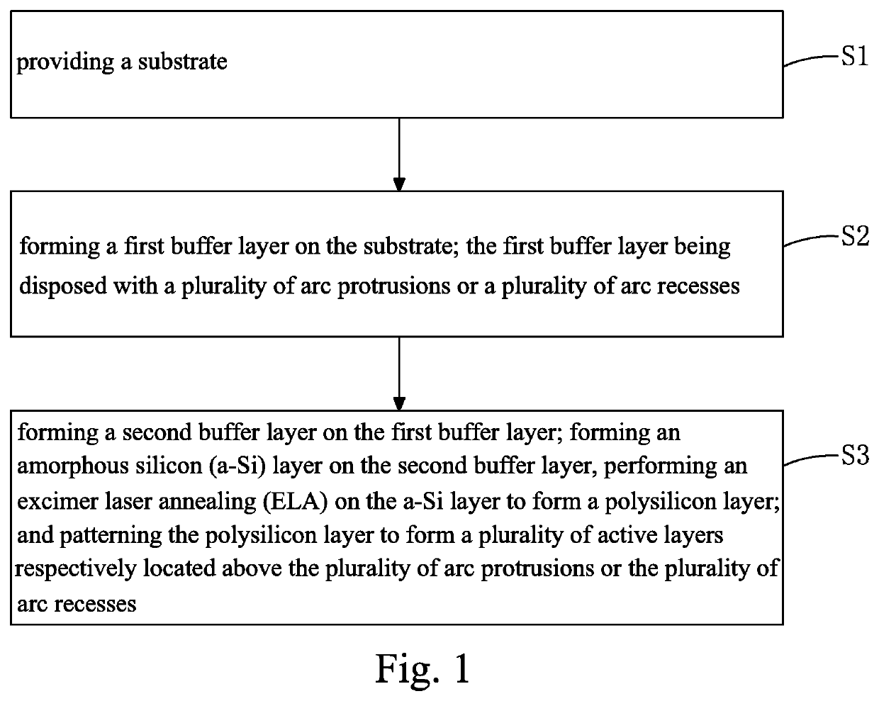
[0043]Refer to FIG. 1, as well as FIG. 2 to FIG. 11. The manufacturing method for TFT array substrate of the present invention comprises the following steps:

[0044]Step S1: as shown in FIG. 2, providing a substrate 10.

[0045]Specifically, the substrate 10 can be made of glass or a flexible material.

[0046]Step S2: as shown in FIG. 6, forming a first buffer layer 20 on the substrate 10. The first buffer layer 20 is disposed with a plurality of arc protrusions 21.

[0047]Specifically, the material for the first buffer layer 20 can be SiNx, SiOx, or other materials often used as buffer layer in the TFT array substrate.

[0048]Specifically, the first buffer layer is made of a material of silicon nitride or silicon oxide and has a thickness of 3000-8000 Å, and preferably, 5000 Å.

[0049]Specifically, in the first embodiment of the present invention, the first buffer layer 20 having a plurality of arc protrusions 21 is formed by a lithographic process and etching. Of course, in other embodiments o...

second embodiment

[0063]Specifically, in the present invention, the first buffer layer 20 having a plurality of arc recesses 22 is formed by a lithographic process and etching. Of course, in other embodiments of the present invention, other methods for forming recesses on a film layer commonly used in the prior art may also be used to form the first buffer layer 20.

[0064]Moreover, in the second embodiment of the present invention, in step S2, the use of the lithographic process with etching to form the first buffer layer 20 on the substrate 10 specifically comprises:

[0065]First, referring to FIG. 12, forming a buffer material layer 29 on the substrate 10; coating a positive photoresist material on the buffer material layer 29 to form a photoresist material layer 90′.

[0066]Then, referring to FIG. 12, providing a halftone mask (HTM) 100′ comprising a plurality of spaced semi-transmissive regions 110′ and a fully-transmissive region 120′ outside the semi-transmissive region 110′; in the semi-transmissiv...


PUM

PropertyMeasurementUnit
thicknessaaaaaaaaaa
transmittanceaaaaaaaaaa
energyaaaaaaaaaa

Abstract

The invention provides a manufacturing method for TFT array substrate and TFT array substrate. The manufacturing method forms a first buffer layer on the substrate; the first buffer layer is disposed with a plurality of arc protrusions or a plurality of arc recesses; then an a-Si layer is formed on the second buffer layer which is formed on the first buffer layer; in the process of forming a polysilicon layer by performing ELA on the a-Si layer, the arc protrusions or the arc recesses can change the optical path of the laser to form an energy gradient in the a-Si layer, so as to increase the grain size in the formed polysilicon layer, reduce the number of grain boundaries, improve the carrier mobility of the TFT device, and improve the electrical properties of the TFT device.

Description

BACKGROUND OF THE INVENTION1. Field of the Invention[0001]The present invention relates to the field of display, and in particular to a thin film transistor (TFT) array substrate and liquid crystal display (LCD).2. The Related Arts[0002]In the field of display technology, a panel display device, such as liquid crystal display (LCD), organic light-emitting diode (OLED) display device, has gradually replaced a cathode ray tube (CRT) display device. The LCD has many advantages such as thinness, power saving, no radiation, and so on, and has been widely used.[0003]A conventional display device is generally provided with a thin film transistor (TFT) array substrate as a driving structure, and the TFT array substrate comprises a plurality of TFT devices arranged in an array. The performance of the TFT array substrate greatly affects the quality of the display device. With the continuous development of panel display technology, high-resolution and low-energy display devices are increasingl...

Claims


Application Information

Patent Timeline
Patent Type & Authority Patents(United States)
IPC IPC(8): H01L21/00H01L27/12H01L21/268
CPCH01L21/268H01L27/1285H01L27/1288H01L27/1222H01L21/02422H01L21/02488H01L21/02494H01L21/02502H01L21/02532H01L21/02686H01L27/1218H01L27/1262H01L29/66757H01L29/78603H01L29/78621H01L29/78675
Inventor ZHANG, RUIJUNWANG, SONG
Owner TCL CHINA STAR OPTOELECTRONICS TECH CO LTD
Features
  • R&D
  • Intellectual Property
  • Life Sciences
  • Materials
  • Tech Scout
  • Unparalleled Data Quality
  • Higher Quality Content
  • 60% Fewer Hallucinations
Learn More