Display device and manufacturing method thereof

a technology of display panel and manufacturing method, which is applied in the direction of semiconductor devices, instruments, optics, etc., can solve the problems of uneven brightness of display panel, and achieve the effect of reducing optical distan

Active Publication Date: 2020-05-26
INTERFACE TECH CHENGDU CO LTD +2
View PDF9 Cites 2 Cited by
  • Summary
  • Abstract
  • Description
  • Claims
  • Application Information

AI Technical Summary

Benefits of technology

[0017]In the aforementioned embodiments of the present disclosure, since the optical particles of a material including silicon or epoxy resin are first uniformly mixed with the optical adhesive including silicon or poly(methyl methacrylate) at a suitable ratio to form the colloid having a function of light diffusion. Subsequently, the colloid including the optical particles is coated on the surface of the substrate, such that the colloid is sufficiently filled in the gaps between the light emitters, so that the areas between the light emitters that cannot emit light can reflect the light of the light emitters by being filled with the colloid. This leads to forming a continuous light-emitting area to achieve the function of light diffusion. Therefore, when the optical distance is reduced, the situation in which the brightness of the liquid crystal panel is uneven due to the high brightness of the areas of the liquid crystal panel corresponding to the light-emitting range of the light-emitting chip is not caused. In this way, when the optical distance is reduced to a range from 0 mm to 1 mm, the brightness uniformity of the liquid crystal panel can be maintained to successfully achieve the purpose of thinning the display device.

Problems solved by technology

Although reducing the optical distance in the display device contributes to thinning the display device, and since the optical distance is smaller, the positions of liquid crystal panel corresponding to the LED chips have greater brightness; therefore, it is simple to cause a situation in which the brightness of the display panel is uneven.

Method used


Image

  • Display device and manufacturing method thereof
  • Display device and manufacturing method thereof
  • Display device and manufacturing method thereof

Examples


Embodiment Construction

[0024]Reference will now be made in detail to the present embodiments of the disclosure, examples of which are illustrated in the accompanying drawings. Wherever possible, the same reference numbers are used in the drawings and the description to refer to the same or like parts.

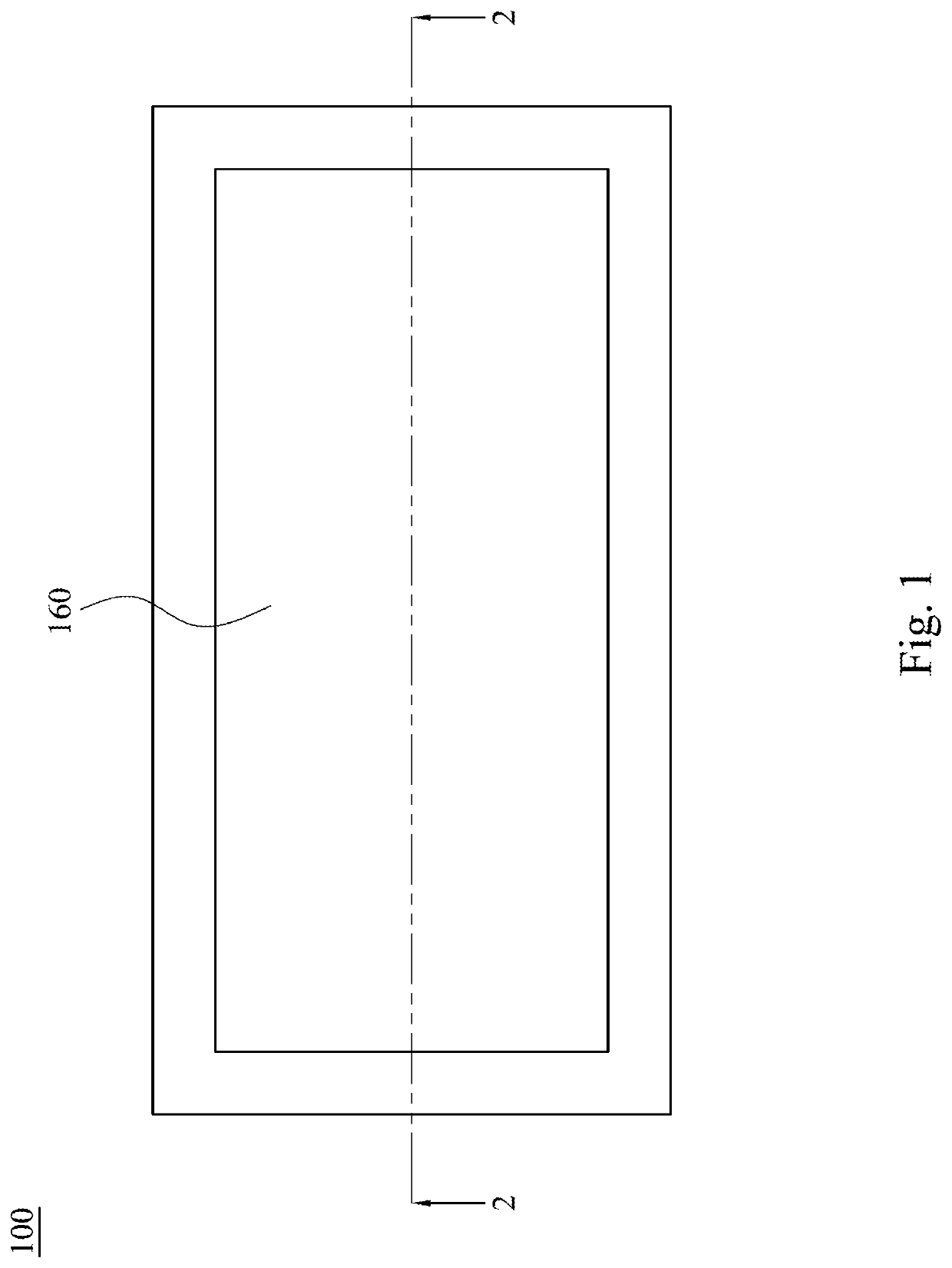
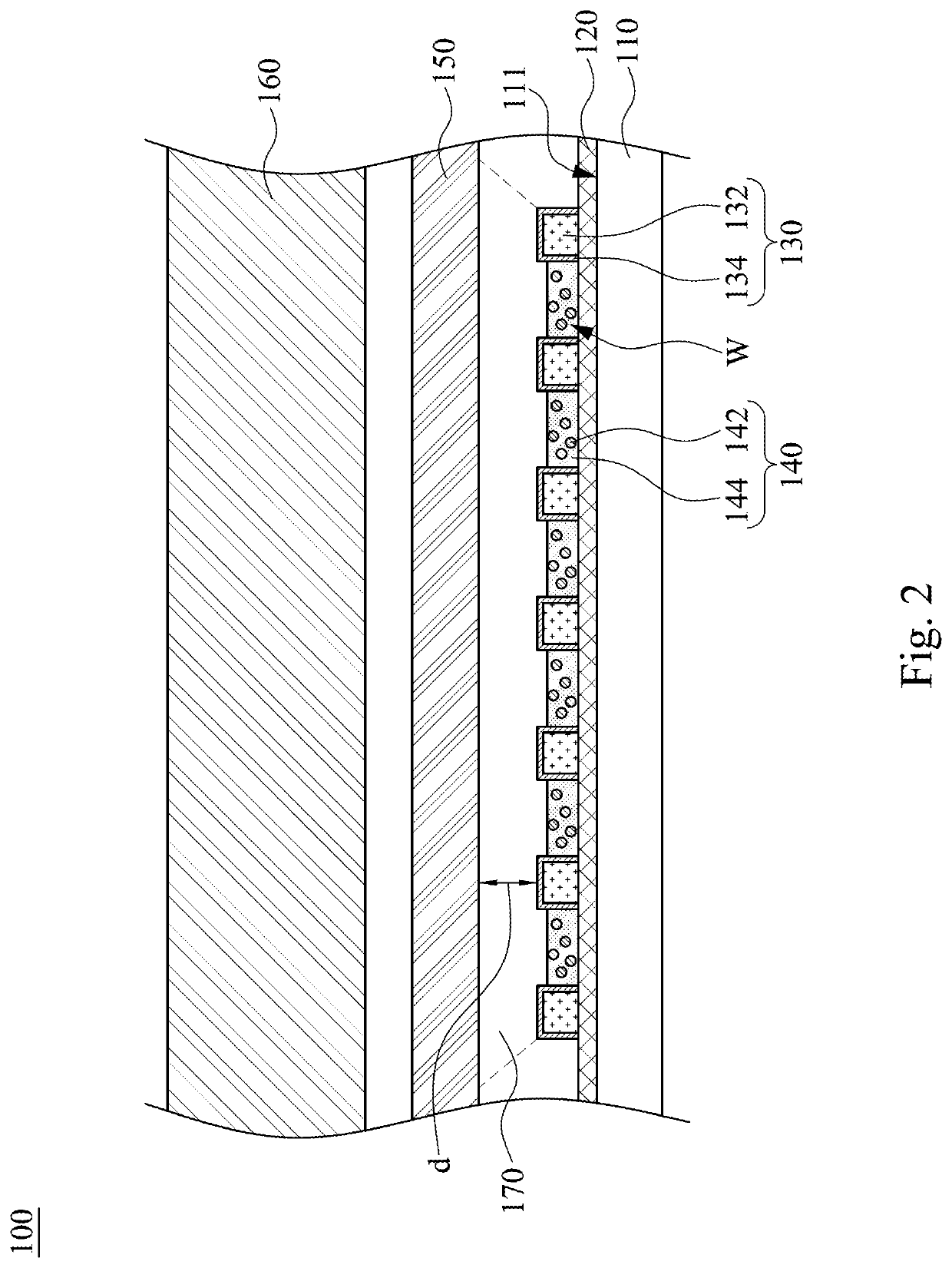
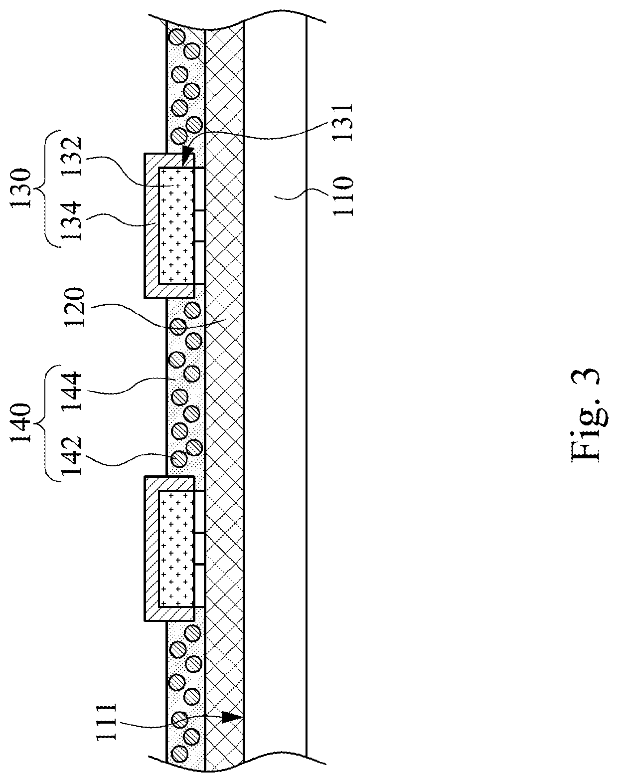
[0025]FIG. 1 illustrates a top view of a display device according to an embodiment of the present disclosure. FIG. 2 illustrates a cross-sectional view of the display device taken along line 2-2 shown in FIG. 1. As shown in FIG. 2, a display device 100 includes a substrate 110, a plurality of light emitters 130, a colloid 140, an optical film 150, and a liquid crystal panel 160. The light emitters 130 are located on a surface 111 of the substrate 110. There are a plurality of gaps W between the adjacent light emitters 130. The colloid 140 is located in the gaps W on the surface 111 of the substrate 110 and surrounds the light emitters 130. The optical film 150 is located above the light emitters 130. The liqu...


PUM

PropertyMeasurementUnit
optical distanceaaaaaaaaaa
particle diameteraaaaaaaaaa
sizeaaaaaaaaaa

Abstract

A display device includes a substrate, a plurality of light emitters, a colloid, an optical film, and a liquid crystal panel. The light emitters are located on a surface of the substrate. There are a plurality of gaps between the light emitters. The colloid is located in the gaps on the surface of the substrate and surrounds the light emitters. The optical film is located above the colloid and the light emitters. The liquid crystal panel is located above the optical film.

Description

RELATED APPLICATIONS[0001]This application claims priority to China Application Serial Number 201811494600.2, filed Dec. 7, 2018, which is herein incorporated by reference.BACKGROUNDField of Invention[0002]The present disclosure relates to a display device and a manufacturing method of the display device.Description of Related Art[0003]In the field of display devices, mini light-emitting diodes (Mini LEDs) can be used as backlights for the liquid crystal screen. In order to increase the brightness of the display device, a direct back-lit light source may be used to replace the edge back-lit light source. The wavelength of the light-emitting diode chip in the mini light-emitting diode can be converted by fluorescent powder. For example, the blue light of a blue light-emitting diode chip may be mixed with the yellow light of a yellow fluorescent powder to be converted into white light. The packaging method of a module structure combining the light-emitting diode chip and the fluoresce...

Claims


Application Information

Patent Timeline
Patent Type & Authority Patents(United States)
IPC IPC(8): G02F1/13357G02F1/1333
CPCG02F1/133305G02F1/133621G02F1/133611G02F1/133603G02F1/133606G02F2001/133354G02F2001/133624G02F1/133609G02F1/133607G02F2202/28G02F2203/03G02F1/133612G02F1/133614H01L25/0753G02F1/133354G02F1/133624
Inventor CHEN, YIN-CHENGHUANG, WEN-HSIAOHUANG, TA-JEN
Owner INTERFACE TECH CHENGDU CO LTD
Why Eureka
Try Eureka