Step-down chopper circuit having bypass elements
a step-down chopper and bypass element technology, applied in the direction of dynamo-electric converter control, process and machine control, instruments, etc., can solve problems such as voltage breakdown
- Summary
- Abstract
- Description
- Claims
- Application Information
AI Technical Summary
Benefits of technology
Problems solved by technology
Method used
Image
Examples
first embodiment
[0034]Hereinafter, a power conversion device according to the present invention will be described with reference to the drawings.
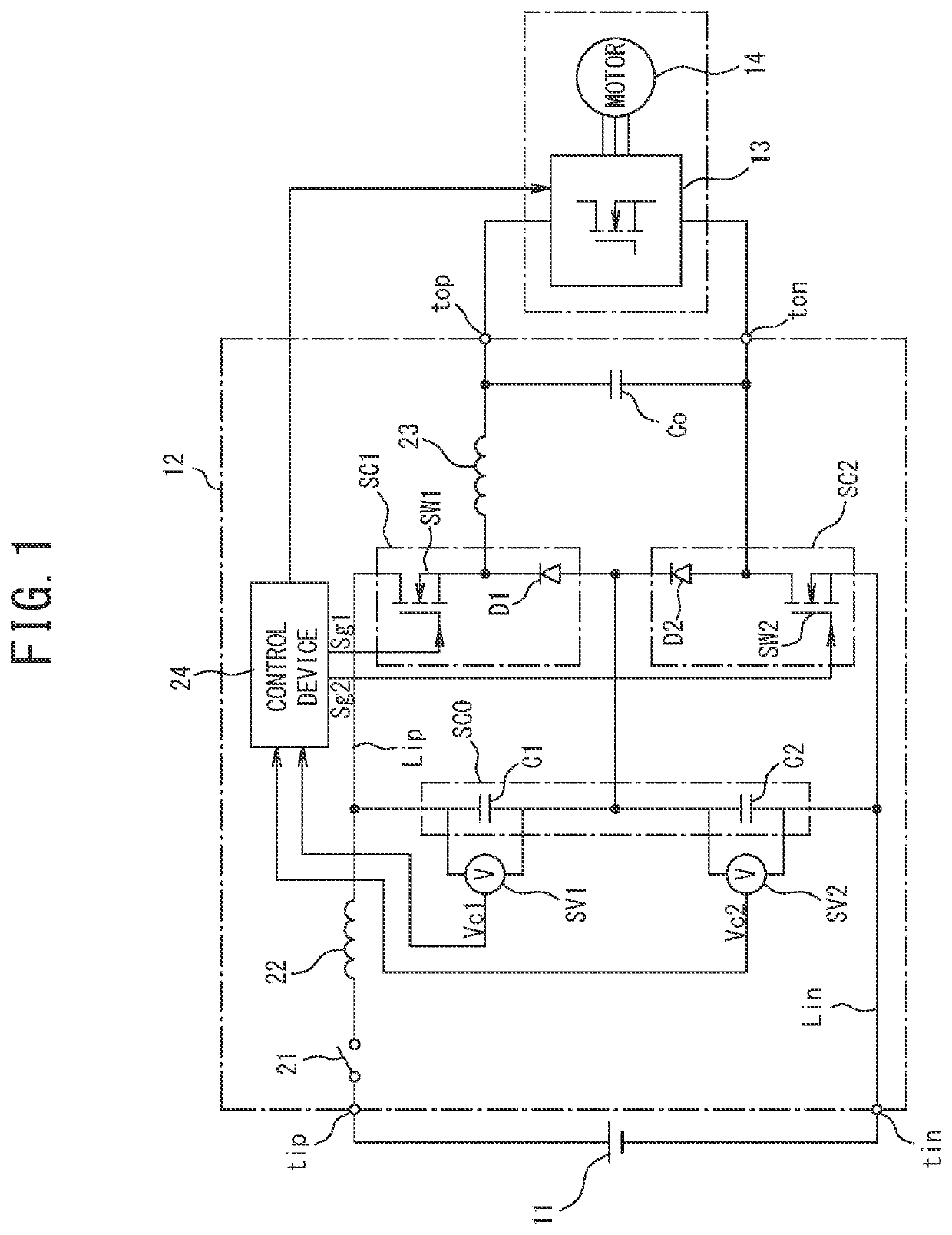
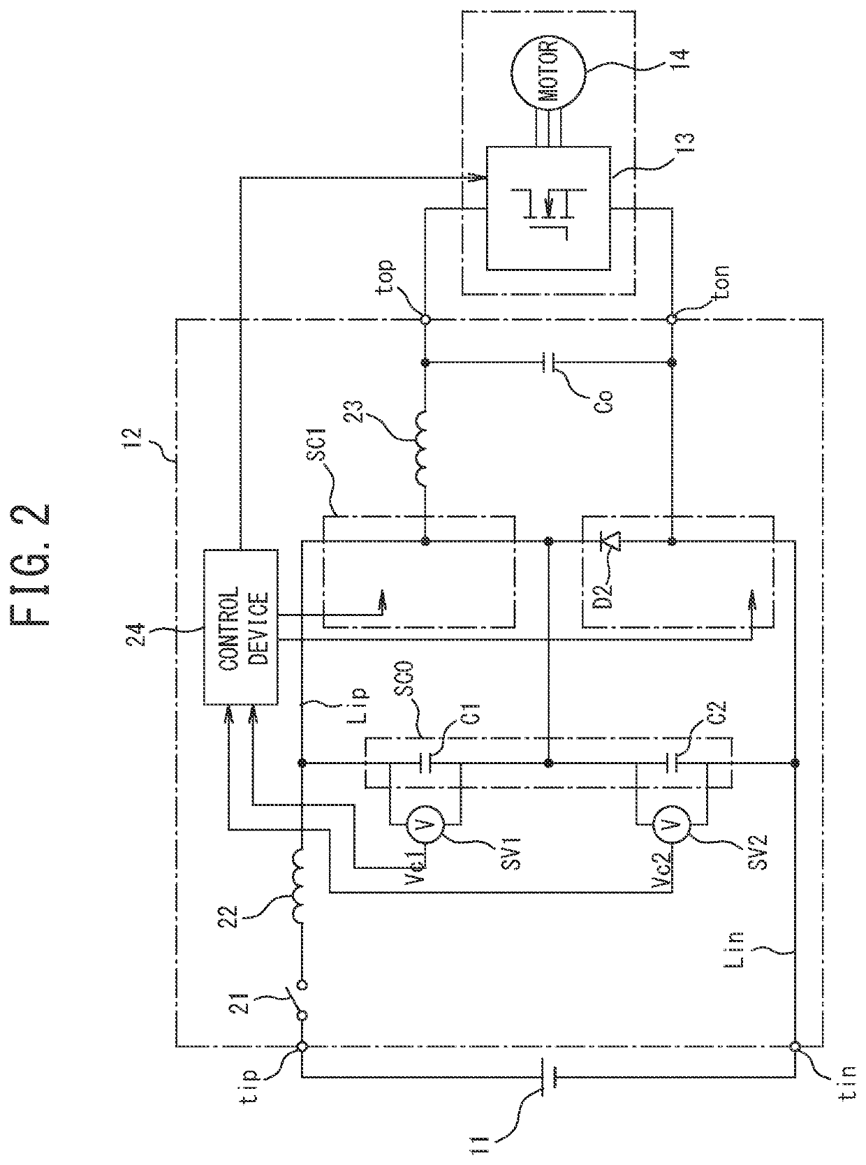
[0035]As illustrated in FIG. 1, the power conversion device includes a DC power supply 11, a step-down chopper circuit 12 configuring a DC-DC converter, an inverter 13, and a load 14 configured by, for example, a motor.
[0036]The step-down chopper circuit 12 includes an input-side positive electrode terminal tip and an input-side negative electrode terminal tin connected to the DC power supply 11, and an output-side positive electrode terminal top and an output-side negative electrode terminal ton connected to the inverter 13. An input-side positive electrode wire (positive electrode-side power wire) Lip and an input-side negative electrode wire (negative electrode-side power wire) Lin are connected to the input-side positive electrode terminal tip and the input-side negative electrode terminal tin. It is to be noted that, in the present embodiment, a curre...
second embodiment
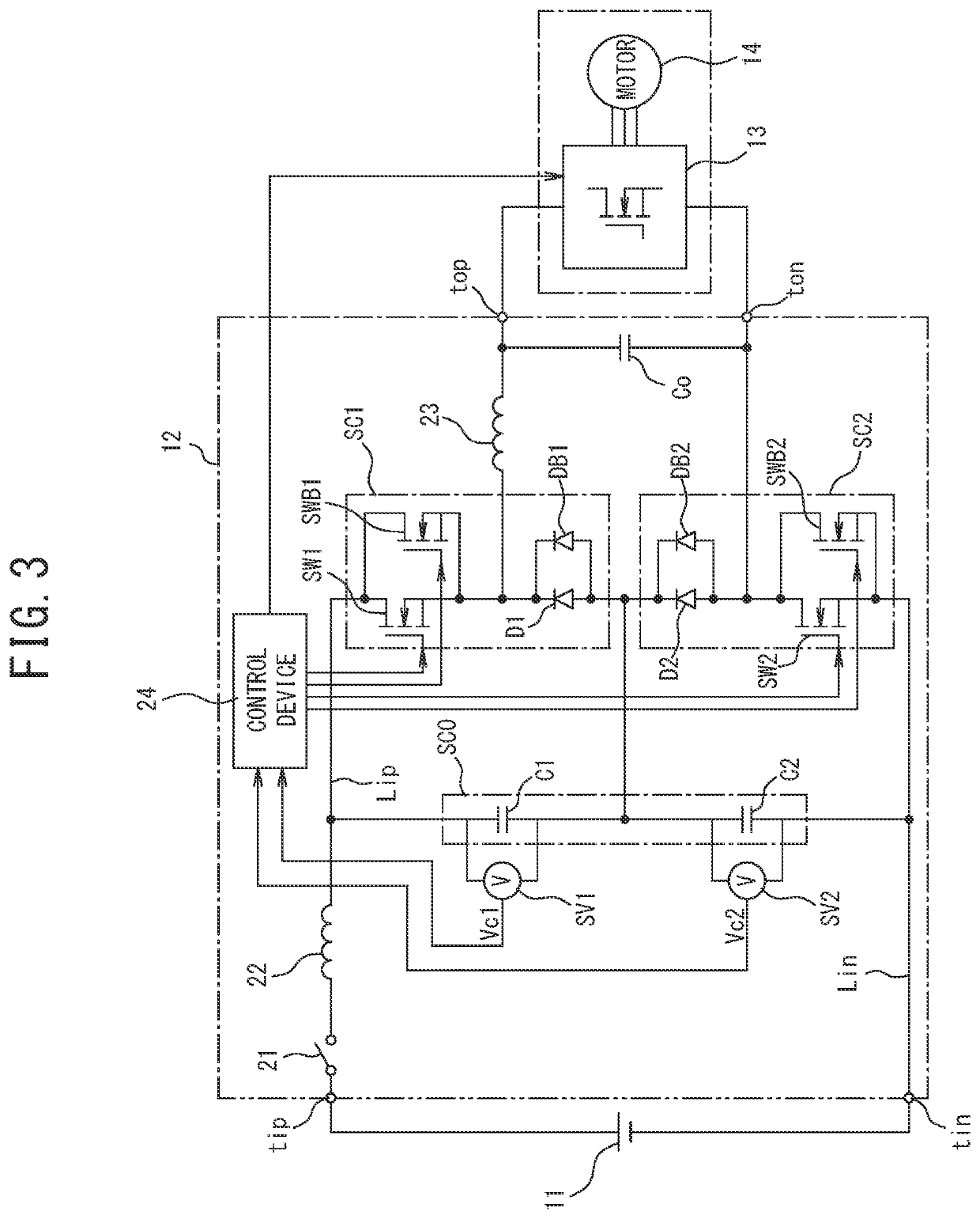
[0068]Next, the present invention will be described with reference to FIG. 3 and FIG. 4.
[0069]In the second embodiment, the formation of the bypass current paths with respect to the capacitors is changed.
[0070]In the second embodiment, in the first series circuit SC1, the first semiconductor switching element SW1 configured by a wide-bandgap semiconductor element and the backflow prevention first diode D1 configured by a wide-bandgap semiconductor element in the same manner configure a series circuit.
[0071]In addition, the first series circuit SC1 includes a bypass semiconductor switching element SWB1 connected in parallel with the first semiconductor switching element SW1 and a bypass diode DB1 connected in parallel with the first diode D1.
[0072]The bypass semiconductor switching element SWB1 and the bypass diode DB1 are configured by semiconductor elements other than wide-bandgap semiconductor elements. In addition, the bypass diode DB1 is set to have a withstand voltage lower tha...
third embodiment
[0095]Next, the present invention will be described with reference to FIG. 5.
[0096]The third embodiment is configured to be operable as a bidirectional converter in the above-described second embodiment.
[0097]More specifically, in the third embodiment, as illustrated in FIG. 5, in the first series circuit SC1, a boost diode DBo1 is inverse-parallel connected in parallel with the first semiconductor switching element SW1. In addition, a boost semiconductor switching element SWBo1 is connected in parallel with the first diode D1.
[0098]In addition, in the second series circuit SC2, a boost semiconductor switching element SWBo2 is connected in parallel with the second diode D2. In addition, a boost diode DBo2 is inverse-parallel connected in parallel with the second semiconductor switching element SW2.
[0099]Here, the boost semiconductor switching elements SWBo1 and SWBo2 are set to have withstand voltages lower than the withstand voltages of the first capacitor C1 and the second capacit...
PUM
| Property | Measurement | Unit |
|---|---|---|
| current | aaaaa | aaaaa |
| withstand voltage | aaaaa | aaaaa |
| voltage | aaaaa | aaaaa |
Abstract
Description
Claims
Application Information


