
Semiconductor programmable device

a programmable device and semiconductor technology, applied in semiconductor devices, diodes, electrical equipment, etc., can solve problems such as defect-free packaging chips, often replaced defective devices, and repair is no longer possible, so as to prevent voltage breakdown

Inactive Publication Date: 2005-05-19
U CHIP TECH
View PDF1 Cites 0 Cited by
  • Summary
  • Abstract
  • Description
  • Claims
  • Application Information

AI Technical Summary

Benefits of technology

[0013] Accordingly, at least one objective of the present invention is to provide a semiconductor programmable device that can be activated using a lower control voltage to prevent a voltage breakdown.
[0014] A second objective of this invention is to provide a semiconductor programmable device with an identical transistor and capacitor gate oxide layer thickness so that the fabrication process can be simplified and the production cost can be reduced.
[0017] In this invention, a PMOS transistor is used instead of the conventional NMOS transistor to prevent possible unexpected operations in other devices on the chip when too large a control voltage is applied as well as voltage breakdown. Furthermore, because both the transistor and the capacitor gate oxide layer has an identical thickness, the process of fabricating the semiconductor programmable device is simplified so that overall production cost is reduced.

Problems solved by technology

Thus, the most important issue facing the semiconductor industry is to develop ways for increasing overall yield of the product.
In the earlier type of backup systems, defective devices are often replaced by the backup devices.
For a chip using this repair technique, repair is no longer possible after the chip has been packaged.
Yet, a packaged chip may not be defect free.
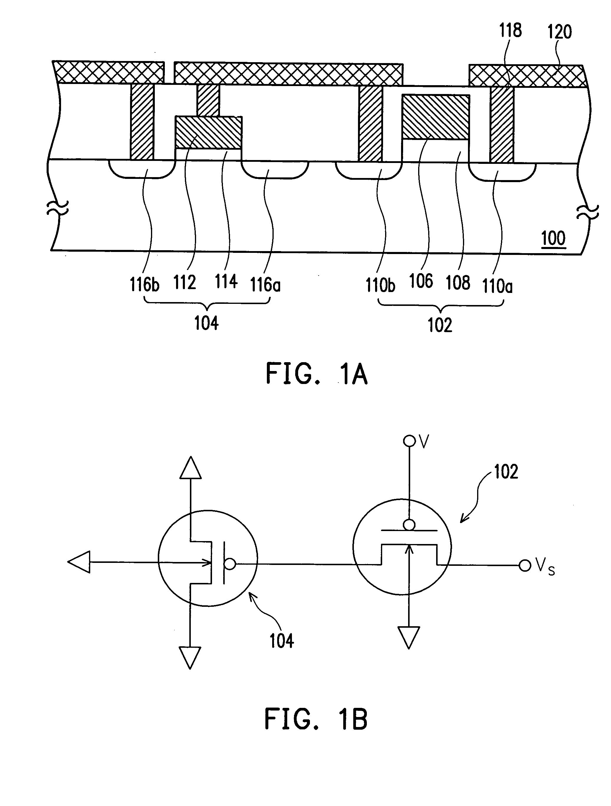
With the application of a relative high control voltage V, it is possible to cause a punch through of the gate oxide layer 106 of the NMOS transistor 102 leading to a short circuit failure of the entire device.
However, producing the gate oxide layer 106 and the gate oxide layer 114 such that each has a different thickness requires a more complicated fabrication process and hence increases overall production cost.
Moreover, the application of a large control voltage V may cause some abnormality in the operation of field devices or a drop in overall device performance.

Method used


Image

  • Semiconductor programmable device
  • Semiconductor programmable device
  • Semiconductor programmable device

Examples


Embodiment Construction

[0024] Reference will now be made in detail to the present preferred embodiments of the invention, examples of which are illustrated in the accompanying drawings. Wherever possible, the same reference numbers are used in the drawings and the description to refer to the same or like parts.

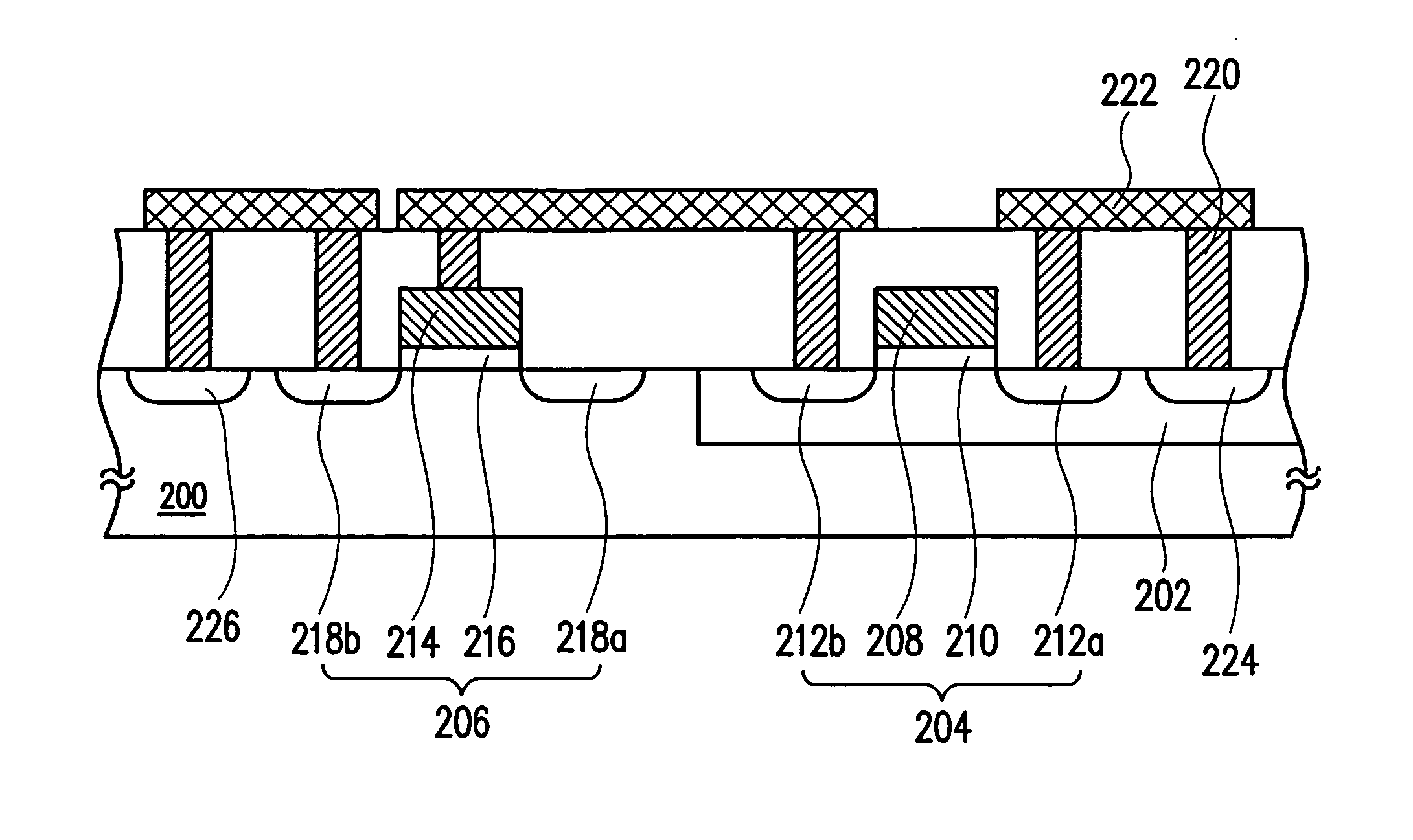
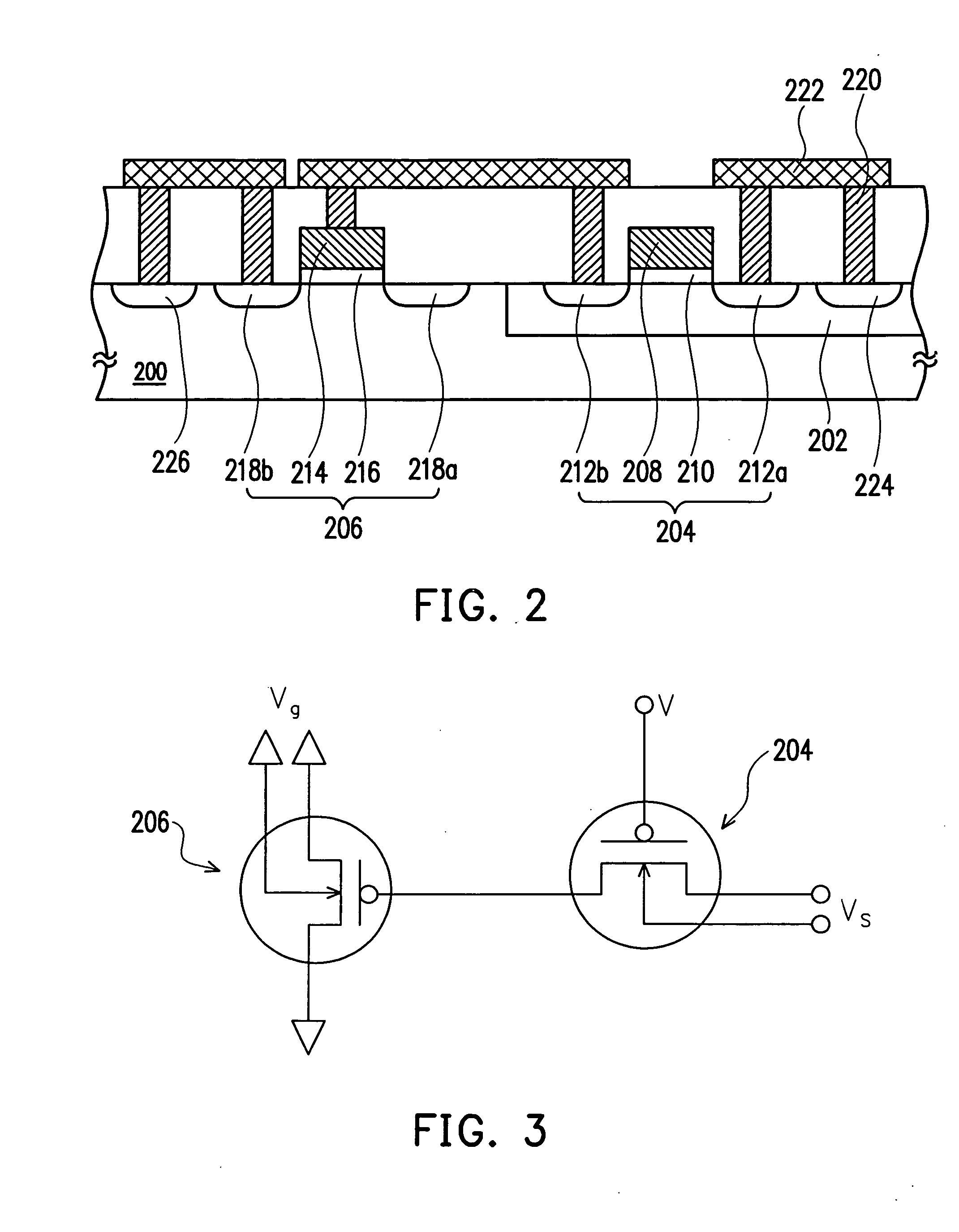
[0025]FIG. 2 is a schematic cross-sectional view of a semiconductor programmable device according to one preferred embodiment of this invention. As shown in FIG. 2, the semiconductor programmable device comprises a P-type substrate 200, an N-well 202, a PMOS transistor 204 and an NMOS capacitor 206. The P-type substrate 200 is a silicon substrate with lightly doped P-type dopants, for example. The N-well 202 is configured within the P-type substrate 200. The N-well 202 is formed, for example, by lightly doping N-type dopants into the P-type substrate in an ion implantation.

[0026] The PMOS transistor 204 has a gate 208, a gate oxide layer 210 and two source / drains' 212a and 212b. The gate oxide lay...


PUM


Abstract

A semiconductor programmable device is provided. The semiconductor programmable device comprises a P-type substrate, an N-well, an NMOS capacitor and a PMOS transistor. The N-well is formed in the P-type substrate. The NMOS capacitor is configured on the P-type substrate. The PMOS transistor is configured on the N-well. A source / drain of the PMOS transistor is electrically connected to a gate of the NMOS capacitor. A control voltage is applied to a gate of the PMOS transistor. A programming voltage is applied to the source / drain of the PMOS transistor. The programming voltage is large enough to cause a breakdown of a gate oxide layer of the NMOS capacitor. The gate oxide layer of the NMOS capacitor has a thickness identical to the gate oxide layer of the PMOS transistor.

Description

CROSS-REFERENCE TO RELATED APPLICATION [0001] This application claims the priority benefit of Taiwan application serial no. 92131930, filed on Nov. 14, 2003. BACKGROUND OF THE INVENTION [0002] 1. Field of the Invention [0003] The present invention relates to a method of fabricating a semiconductor device. More particularly, the present invention relates to a method of fabricating a semiconductor programmable device. [0004] 2. Description of the Related Art [0005] Most semiconductor products are fabricated after conducting a series of complicated processes. Typically, the parameters and operating environment of each process will affect the yield of the product. Thus, the most important issue facing the semiconductor industry is to develop ways for increasing overall yield of the product. [0006] To prevent any significant drop in the quantity of semiconductor chips produced leading to a low product yield, a number of backup devices for repairing any defective devices is often fabricat...

Claims


Application Information

Patent Timeline
Patent Type & Authority Applications(United States)
IPC IPC(8): H01L27/06
CPCH01L27/0629
Inventor CHEN, JUI-LUNGHSU, YANG-CHENWANG, CHIEN-JIUN
Owner U CHIP TECH
Learn More