Method and device for measurement of a plurality of semiconductor chips in a wafer array
a technology of semiconductor chips and arrays, applied in the direction of individual semiconductor device testing, semiconductor/solid-state device testing/measurement, instruments, etc., can solve the problem of increasing the manufacturing cost of semiconductor chips, electrical characteristic values cannot be measured over large areas in a single spatially resolved measurement using today's methods, and the cost of semiconductor chips is increasing. , to achieve the effect of cost-effective and efficient measurement of semiconductor chips
- Summary
- Abstract
- Description
- Claims
- Application Information
AI Technical Summary
Benefits of technology
Problems solved by technology
Method used
Image
Examples
first embodiment
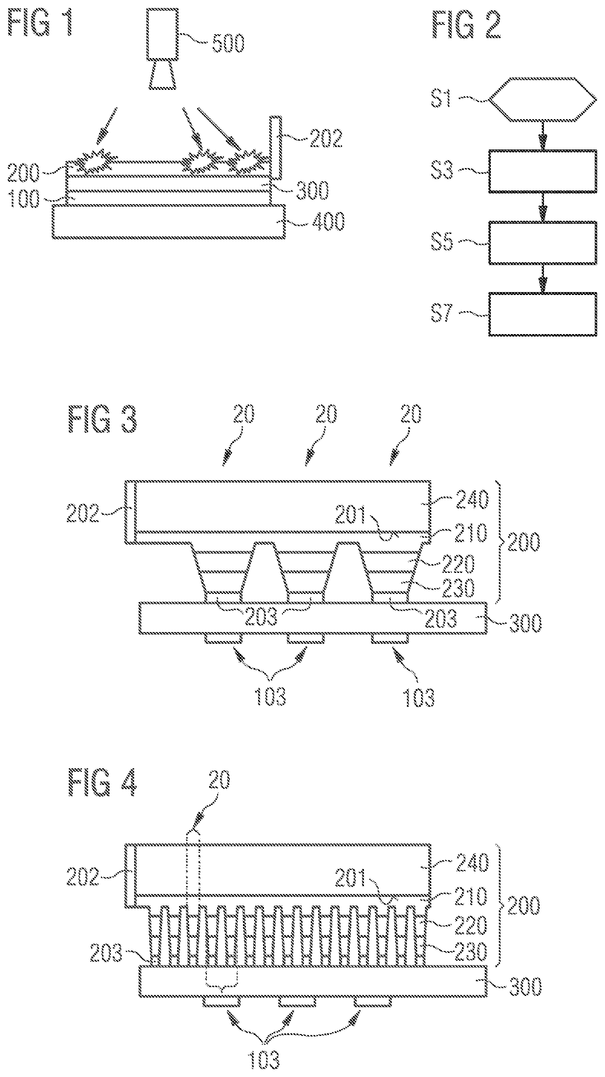
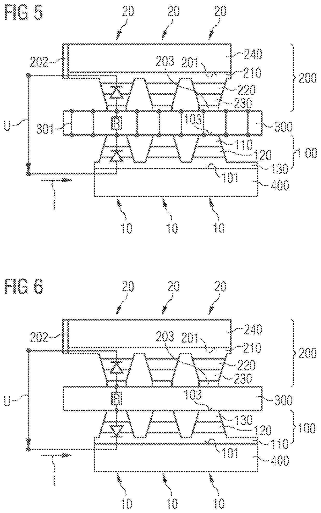
>FIG. 1 shows a first embodiment for the measurement of a plurality of semiconductor chips in the wafer array. A wafer array 100 to be measured with a plurality of semiconductor chips 10 (see FIGS. 5-7b) is arranged on a carrier 400, for example, a metal chuck. The wafer array 100 is then brought into contact with a conductive layer 300 of polymer and a contact structure 200 across the entire surface. The contact structure 200 can also be described as a so-called “probe wafer”. A voltage is then applied between the carrier 400 and the contact structure 200, for example, via a side contact 202. The contact structure 200 comprises a plurality of measurement semiconductor chips 20 (see FIGS. 2-6), which then emit radiation which is detected in spatial resolution by a camera system 500.
[0080]Using the exemplary flow chart in FIG. 2, the method steps for measurement of the semiconductor chips 10 according to FIG. 1 are explained in more detail below.
[0081]In a step S1, the wafer composit...
second embodiment
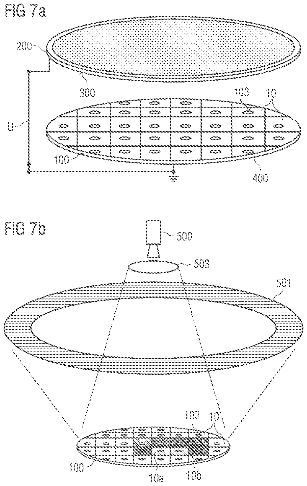
[0092]FIGS. 7a and 7b show a second embodiment for the measurement of a plurality of semiconductor chips 10 in the wafer array 100. The wafer array 100 is arranged on a carrier 400 and the semiconductor chips 10 are contacted over their entire surface by means of a conductive layer 300 of rubber, which is applied to a contact structure 200 designed as a metal chuck (FIG. 7a). Then a counter voltage pulse of, e.g., −100 V is applied for 10 s between the contact structure 200 and the carrier 400. Due to the parallel connection, all semiconductor chips 10 are subjected to the same load. In semiconductor chips 10 with reverse weakness, a current of about 4 mA flows, which generates a shunt and thereby damages the semiconductor chips. The current flowing locally can be adjusted by the conductivity of the rubber, which is a series resistance. In this context, such an energy input into the semiconductor chip 10 can be set that the shunt generated is large enough to be detected in a subsequ...
PUM
| Property | Measurement | Unit |
|---|---|---|
| thickness | aaaaa | aaaaa |
| thickness | aaaaa | aaaaa |
| voltage | aaaaa | aaaaa |
Abstract
Description
Claims
Application Information


