Glitch removal circuit and electronic device

a technology of electronic devices and circuits, applied in pulse techniques, voltage/temperature variation compensation, reliability increasing modifications, etc., can solve problems such as the glitch removal circuit not being able to operate normally, and achieve the effect of removing the glitch noise contained

Active Publication Date: 2021-01-26
FANUC LTD
View PDF3 Cites 0 Cited by
  • Summary
  • Abstract
  • Description
  • Claims
  • Application Information

AI Technical Summary

Benefits of technology

[0009]The glitch removal circuit according to an aspect of the present disclosure can remove glitch noise contained in a Power-on Reset signal.

Problems solved by technology

However, in the case of glitch noise being contained in the Power-on Reset signal which initializes the glitch removal circuit made using flip flop, there is concern over the glitch removal circuit not being able to operate normally.

Method used


Image

  • Glitch removal circuit and electronic device
  • Glitch removal circuit and electronic device
  • Glitch removal circuit and electronic device

Examples


Embodiment Construction

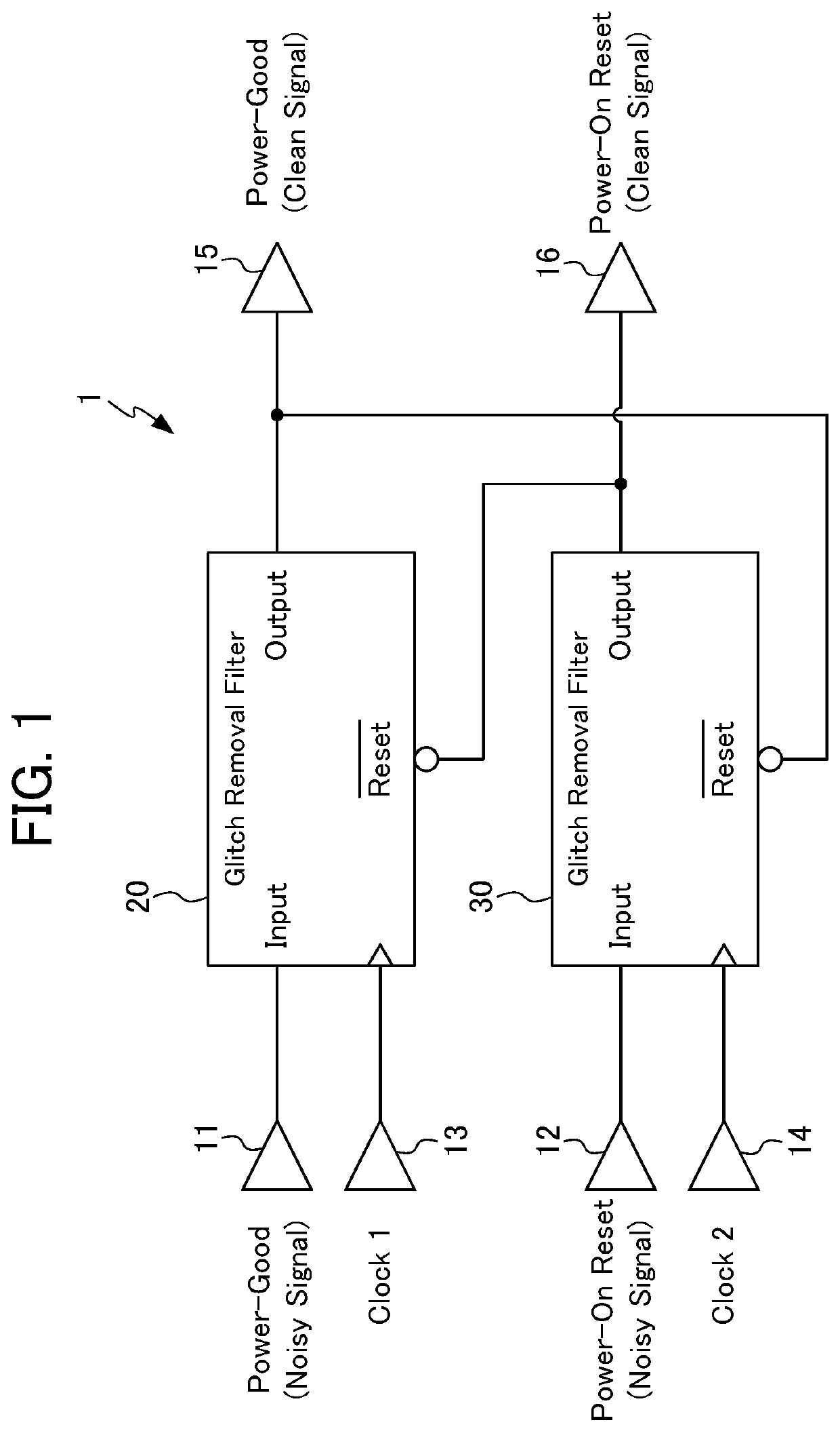
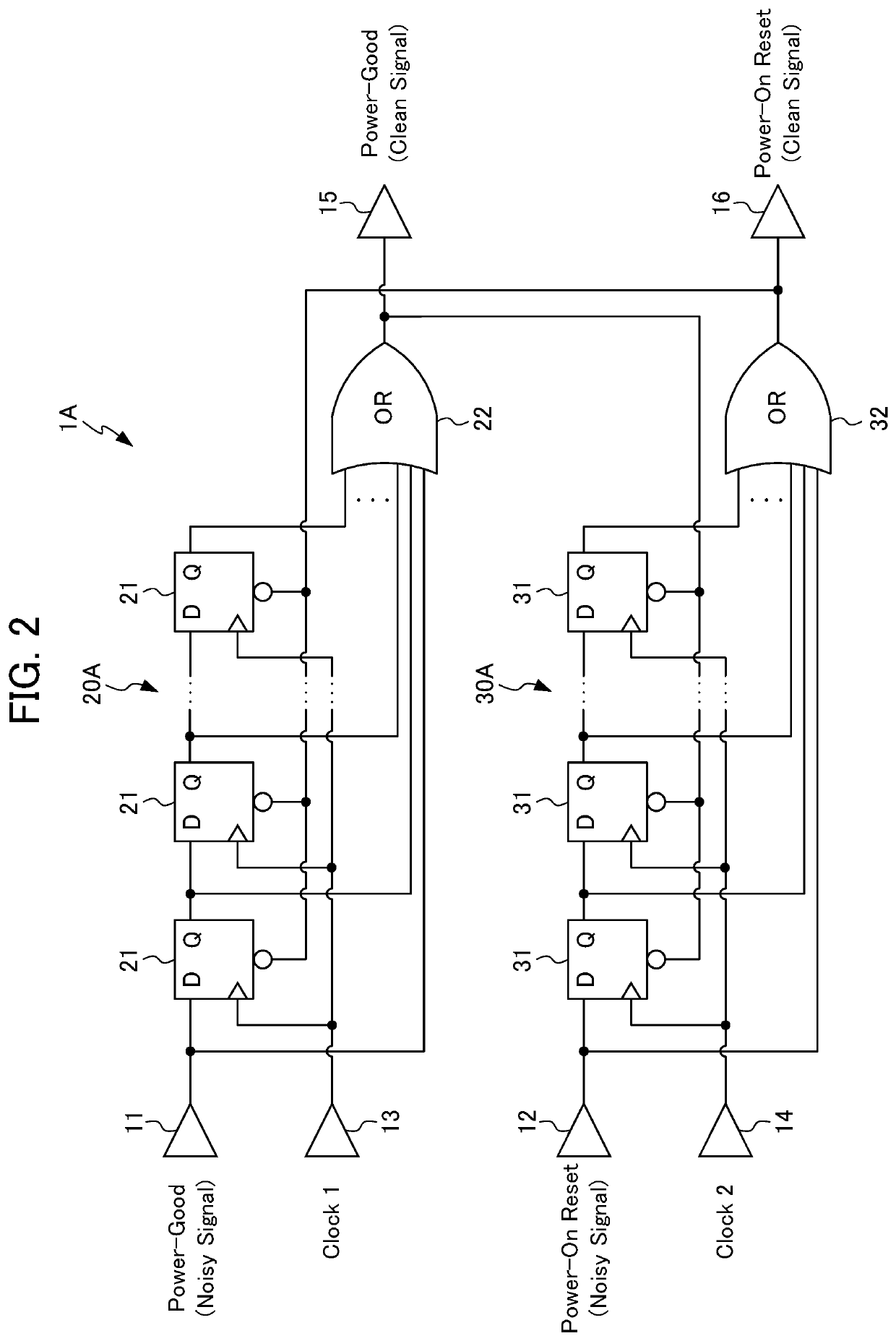
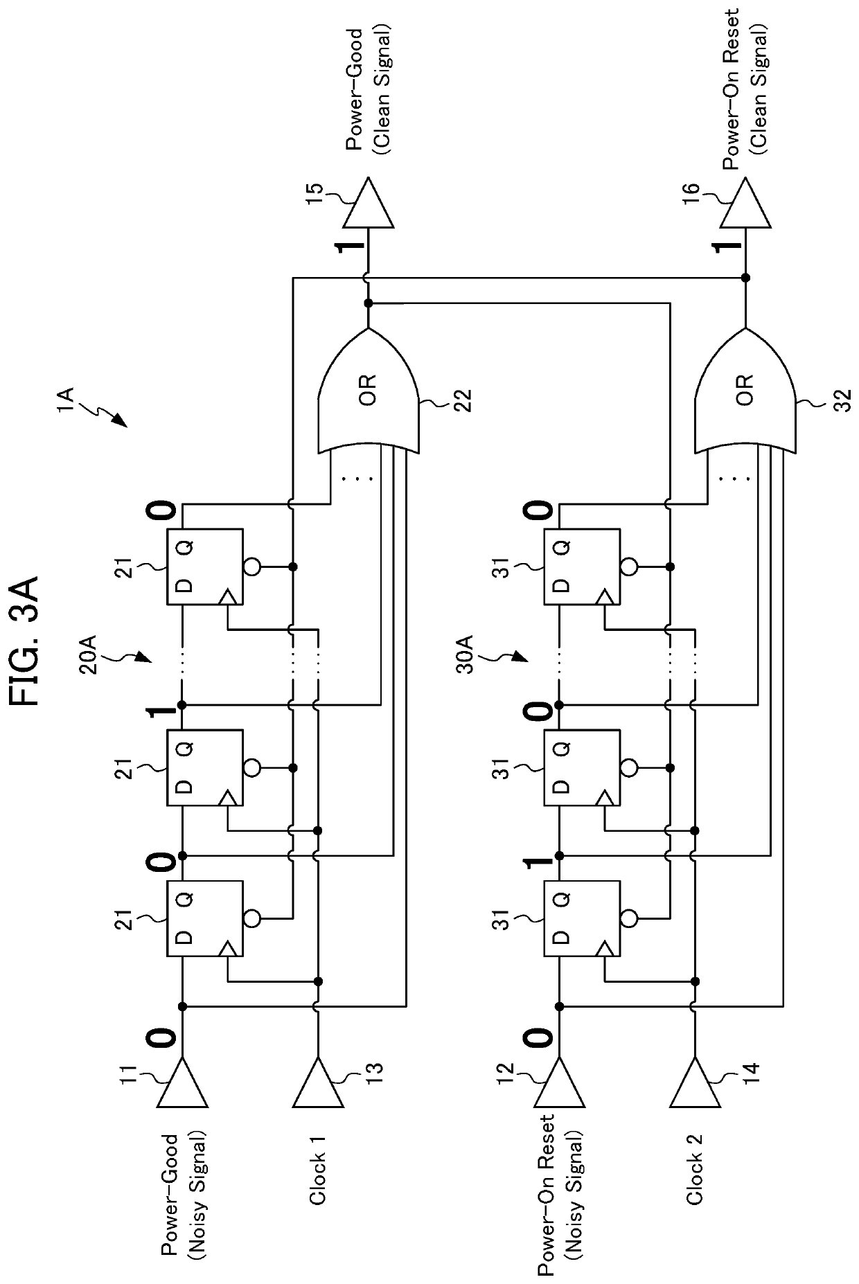
[0042]Hereinafter, an embodiment of the present disclosure will be explained while reference the drawings. FIG. 1 is a circuit diagram showing a glitch removal circuit 1 according to a first embodiment of the present disclosure. The glitch removal circuit 1 removes glitch noise contained in a Power-good signal and Power-on Reset signal. It should be noted that, in the following explanation, “glitch noise” may be explained simply as “glitch”.

[0043]The glitch removal circuit 1 includes: a first input terminal 11 to which an original signal of the Power-good signal (signal which may include glitch noise) is inputted; a second input terminal 12 to which a original signal of the Power-on Reset signal (signal which may include glitch noise) is inputted; a first clock terminal 13 to which a cyclic first clock signal is inputted; a second clock terminal 14 to which a cyclic second clock signal is inputted; a first glitch removal unit 20 which operates according to the first clock signal and...


PUM


Abstract

A glitch removal circuit removes glitch noise contained in a Power-good signal and a Power-on Reset signal, and includes: a first glitch removal unit that operates according to a first clock signal, and removes glitch noise from a Power-good signal; and a second glitch removal unit that operates according to a second clock signal, and removes glitch noise from a Power-on Reset signal, in which the first glitch removal unit is configured so as to be initialized according to an output signal of the second glitch removal unit, and the second glitch removal unit is configured so as to be initialized according to an output signal of the first glitch removal unit.

Description

[0001]This application is based on and claims the benefit of priority from Japanese Patent Application No. 2019-036357, filed on 28 Feb. 2019, the content of which is incorporated herein by reference.BACKGROUND OF THE INVENTIONField of the Invention[0002]The present invention relates to a glitch removal circuit and an electronic device.Related Art[0003]In electrical circuits, pulse noise of a whisker shape shorter than the normal pulse width is called a glitch. In logical circuits, if two input signals change in adjacent times, glitches may occur in the output. This is a phenomenon caused by the signal delay time of two signals, and is called racing.[0004]In addition, when a plurality of output terminals in an integrated circuit or the like changes in the same direction simultaneously, racing may occur in adjacent terminals, and this is called simultaneous switching noise. As a separate example, in the case of there being two signals running parallel, a glitch may occur in the other...

Claims


Application Information

Patent Timeline
Patent Type & Authority Patents(United States)
IPC IPC(8): H03K5/1252H03K5/135H03K19/003
CPCH03K5/1252H03K5/135H03K19/00369H03K5/07H03K5/08
Inventor KOMATSU, TAKAAKI
Owner FANUC LTD
Why Eureka
Try Eureka